
Electrostatic discharge protection circuit

An electrostatic discharge protection and circuit technology, which is applied to emergency protection circuit devices, emergency protection circuit devices for limiting overcurrent/overvoltage, circuits, etc., can solve the problems of occupying layout area, increase efficiency and reduce capacitance The effect of load

Active Publication Date: 2013-03-06
FARADAY TECH CORP
View PDF6 Cites 5 Cited by
  • Summary
  • Abstract
  • Description
  • Claims
  • Application Information

AI Technical Summary

Problems solved by technology

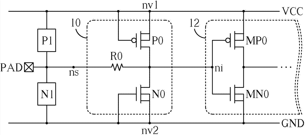
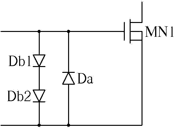
This reverse diode takes up additional layout area

Method used


Image

  • Electrostatic discharge protection circuit
  • Electrostatic discharge protection circuit
  • Electrostatic discharge protection circuit

Examples


Embodiment Construction

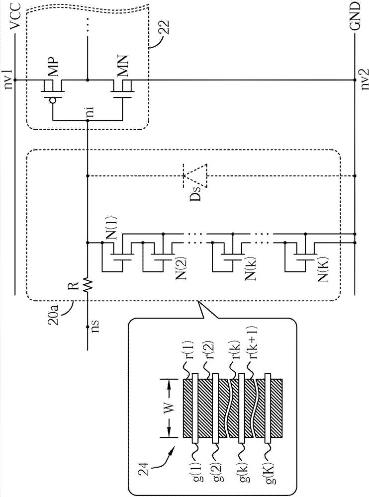
[0028] Please refer to figure 2 , which shows an electrostatic discharge protection circuit 20a according to an embodiment of the present invention, which can be disposed in a chip to protect the internal circuit 22 in the chip. For example, the internal circuit 22 may include a transistor MP and a transistor MN, which are n-channel and p-channel metal-oxide-semiconductor transistors respectively. (signal node) on the signal winding to receive the signal. The signal source can come from an input pad, or be coupled to node ns by a signal output from a different power domain. The internal circuit 22 is respectively coupled to the voltage VCC (power supply voltage) and GND (ground voltage) by the power windings of the nodes nv1 and nv2 (the two nodes can be regarded as voltage nodes); the source and bulk of the transistor MN are It is coupled to the node nv2, and the source and body of the transistor MP are coupled to the node nv1. Transistors MN and MP can be thin-oxide tran...


PUM


Abstract

The invention discloses an electrostatic discharge protection circuit which is provided with a resistor and at least one protective transistor. The resistor is coupled between an output / input signal node and an internal node of an internal circuit, the protective transistors are connected between a voltage node and the internal node in serial, and grid electrodes of the protective transistors are coupled with drain electrodes thereof. Voltage of the electrostatic discharge protection circuit when triggered and conducted can be reduced effectively, capacitive load on signal windings can be decreased, and application efficiency of arrangement area can be increased.

Description

technical field [0001] The present invention relates to an electrostatic discharge protection circuit, and in particular to an electrostatic discharge protection circuit based on a series structure of metal oxide semiconductor transistors. Background technique [0002] Chips are the most important hardware foundation of the modern information society. In order to draw the power required for operation, the chip is equipped with power pads, such as power pads and ground pads, which respectively transmit the operating voltage and ground voltage to the power winding and ground winding in the chip (collectively referred to as power winding). In order to exchange signals with external circuits, the chip is also equipped with input and output pads, which transmit the input and output signals to the signal windings in the chip, so that the internal circuits in the chip can exchange signals through the signal windings. The chip can also be divided into different power domains. The ...

Claims


Application Information

Patent Timeline
Patent Type & Authority Applications(China)
IPC IPC(8): H02H9/04H01L27/02
Inventor 蔡富义彭彦华蔡佳谷柯明道
Owner FARADAY TECH CORP
Learn More