Manufacture method of isolation type power transistor
A technology for power transistors and manufacturing methods, applied in semiconductor/solid-state device manufacturing, electrical components, circuits, etc., can solve problems affecting chip performance, etc., and achieve the effects of low saturation voltage drop, small on-resistance, and high current driving capability
- Summary
- Abstract
- Description
- Claims
- Application Information
AI Technical Summary
Problems solved by technology
Method used
Image
Examples
Embodiment 1
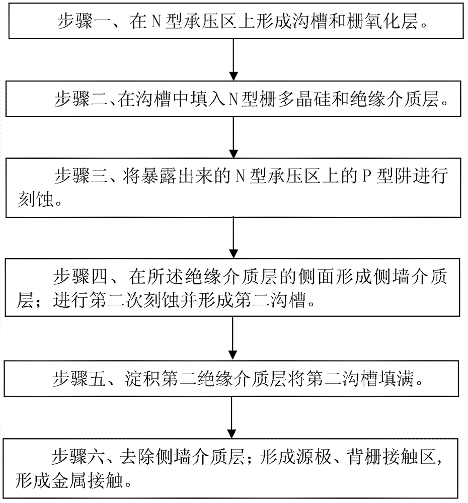
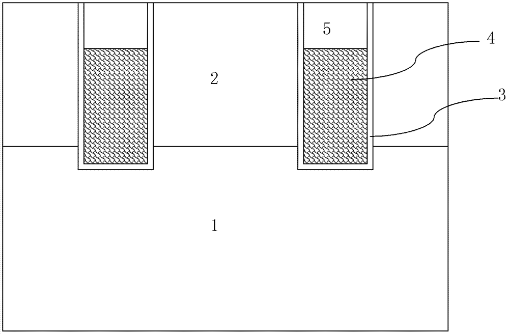
[0036] Such as figure 1 Shown is a flow chart of a method of the embodiment of the present invention; as Figure 2 to Figure 7C Shown is a schematic diagram of the device structure in each step of the method of Embodiment 1 of the present invention. Embodiment 1 of the present invention Manufacturing method of an isolated power transistor The gate of the isolated power transistor prepared has a trench structure, and the method of Embodiment 1 of the present invention includes the following steps:
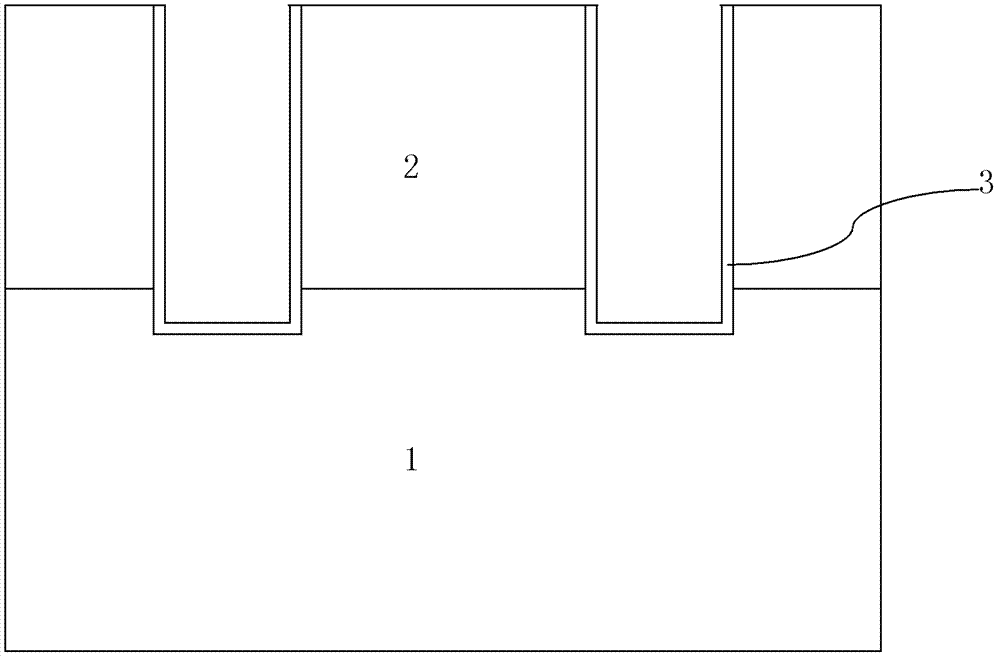
[0037] Step 1, such as figure 2 As shown, a trench is formed on the N-type pressure-bearing region 1 with a P-type well 2 formed on the top, the groove passes through the P-type well 2 and enters into the N-type pressure-bearing region 1, in the The bottom and sidewall surfaces of the trench form gate oxide layer 3 .
[0038] The isolated power transistor can be a silicon-based device or a compound semiconductor device. When the isolated power transistor is a silicon-based devi...
Embodiment 2
[0049] Such as Figure 8 Shown is the flow chart of the second method of the present invention; as Figure 9 to Figure 13B Shown is a schematic diagram of the device structure in each step of the method of Embodiment 2 of the present invention. The method for manufacturing an isolated power transistor according to Embodiment 2 of the present invention. The gate of the isolated power transistor prepared has a surface-type structure. The method according to Embodiment 2 of the present invention includes the following steps:
[0050] Step 1, such as Figure 9 As shown, a gate oxide layer 103, a gate polysilicon 104 and an insulating dielectric layer 105 are sequentially formed on the surface of the N-type pressure receiving region 101 from bottom to top; the insulating dielectric layer 105 and the gate polysilicon 104 are etched Etching is performed to form the gate, that is, the gate is composed of the etched gate polysilicon 104 .
[0051] The isolated power transistor can b...
PUM
 Abstract
Description
Claims
Application Information
 - R&D
- Intellectual Property
- Life Sciences
- Materials
- Tech Scout
- Unparalleled Data Quality
- Higher Quality Content
- 60% Fewer Hallucinations
Browse by: Latest US Patents, China's latest patents, Technical Efficacy Thesaurus, Application Domain, Technology Topic, Popular Technical Reports.
© 2025 PatSnap. All rights reserved.Legal|Privacy policy|Modern Slavery Act Transparency Statement|Sitemap|About US| Contact US: help@patsnap.com


