SOI (Silicon On Insulator)-BJT (Bipolar Junction Transistor) Bi CMOS (Complementary Metal-Oxide-Semiconductor) integrated device with strain SiGe clip-shaped channel and preparation method thereof

A technology for integrating devices and devices, which is applied in semiconductor/solid-state device manufacturing, electric solid-state devices, semiconductor devices, etc., can solve problems such as threshold voltage drift, large influence, and device size cannot be further reduced, so as to improve electron and hole migration rate, performance-enhancing effects

Inactive Publication Date: 2015-07-01
XIDIAN UNIV
View PDF4 Cites 0 Cited by
  • Summary
  • Abstract
  • Description
  • Claims
  • Application Information

AI Technical Summary

Problems solved by technology

[0005] As the feature size of the device enters the sub-50nm stage, many difficulties are encountered in the research process of the strained Si / SiGe CMOS planar structure: short channel effects, hot carrier effects, etc. make the device size unable to be further reduced; gate oxidation The thinning of the layer thickness leads to the breakdown of the oxide layer, and the tunneling current causes the threshold voltage to drift; the polysilicon depletion effect and the resistance of the polysilicon have an increasing influence on the threshold voltage, etc., all of which make the device and circuit performance unable to continue according to Moore. As the law of development continues to develop, it becomes more important to study devices with new structures.

Method used


Image

  • SOI (Silicon On Insulator)-BJT (Bipolar Junction Transistor) Bi CMOS (Complementary Metal-Oxide-Semiconductor) integrated device with strain SiGe clip-shaped channel and preparation method thereof

Examples


Embodiment 1

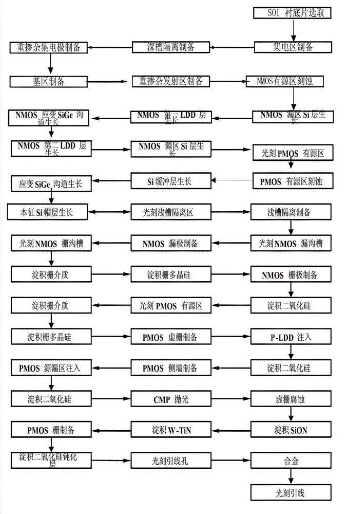
[0112] Embodiment 1: Prepare the SOI BJT, the strained SiGe back channel BiCMOS integrated device and the circuit with the conductive channel of 45nm, the specific steps are as follows:

[0113] Step 1, epitaxial growth.

[0114] (1a) Select the SOI substrate, the support material of the lower layer of the substrate is Si, and the middle layer is SiO 2 , with a thickness of 150nm, and the upper material is doped with a concentration of 1×10 16 cm -3 N-type Si with a thickness of 100nm;

[0115] (1b) Thermally oxidize a layer of SiO with a thickness of 300nm on the substrate surface 2 layer.

[0116] Step 2, isolation area preparation.

[0117] (2a) Epitaxially grow a layer with a doping concentration of 1×10 on the SOI substrate 16 cm -3 A Si layer with a thickness of 0.3 μm acts as a collector area;

[0118] (2b) Thermally oxidize a layer of SiO with a thickness of 200nm on the substrate surface 2 layer;

[0119] (2c) In the photolithographic isolation area, a deep ...

Embodiment 2

[0176] Embodiment 2: prepare SOI BJT, strained SiGe back-channel BiCMOS integrated device and circuit with conductive channel of 30nm, the specific steps are as follows:

[0177] Step 1, epitaxial growth.

[0178] (1a) Select the SOI substrate, the support material of the lower layer of the substrate is Si, and the middle layer is SiO 2 , with a thickness of 300nm, and the upper material is doped with a concentration of 5×10 16 cm -3 N-type Si with a thickness of 120nm;

[0179] (1b) Thermally oxidize a layer of SiO with a thickness of 400nm on the substrate surface 2 layer.

[0180] Step 2, isolation area preparation.

[0181] (2a) Epitaxial growth on SOI substrate with a doping concentration of 5×10 16 cm -3 A Si layer with a thickness of 0.5 μm acts as a collector area;

[0182] (2b) Thermally oxidize a layer of SiO with a thickness of 250nm on the substrate surface 2 layer;

[0183] (2c) In the photolithographic isolation area, a deep trench with a depth of 4 μm ...

Embodiment 3

[0240] Embodiment 3: The SOI BJT, the strained SiGe back channel BiCMOS integrated device and the circuit with the conductive channel of 22nm are prepared, and the specific steps are as follows:

[0241] Step 1, epitaxial growth.

[0242] (1a) Select the SOI substrate, the support material of the lower layer of the substrate is Si, and the middle layer is SiO 2 , with a thickness of 400nm, and the upper material is doped with a concentration of 1×10 17 cm -3 N-type Si with a thickness of 150nm;

[0243] (1b) Thermally oxidize a layer of SiO with a thickness of 500nm on the surface of the substrate 2 layer.

[0244] Step 2, isolation area preparation.

[0245] (2a) Epitaxial growth on SOI substrate with a doping concentration of 1×10 17 cm -3 A Si layer with a thickness of 0.8 μm acts as a collector area;

[0246] (2b) Thermally oxidize a layer of SiO with a thickness of 300nm on the substrate surface 2 layer;

[0247] (2c) In the photolithographic isolation area, a d...


PUM

PropertyMeasurementUnit
thicknessaaaaaaaaaa
thicknessaaaaaaaaaa
thicknessaaaaaaaaaa

Abstract

The invention discloses a preparation method of an SOI (Silicon On Insulator)-BJT (Bipolar Junction Transistor) Bi CMOS (Complementary Metal-Oxide-Semiconductor) integrated device with a strain SiGe clip-shaped channel and a circuit. The preparation process is as follows: preparing a buried layer on an SOI (Silicon On Insulator) substrate sheet, growing an N type Si epitaxy, preparing a deep-trench isolator, and manufacturing a conventional Si bipolar transistor in the bipolar device region; respectively and continuously growing an N type Si epitaxial layer, an N type strain SiGe layer and the like on the active regions of a substrate NMOS (N-Channel Metal Oxide Semiconductor) device and a substrate PMOS (P-Channel Metal Oxide Semiconductor) device at 600 DEG C-780 DEG C, and respectively preparing a drain electrode, a grid electrode and a source region on the active region of the NMOS device to prepare the NMOS device; depositing SiO2 and Poly-Si on the active region of the PMOS device to prepare a virtual grid electrode, depositing a medium layer to form a grid wall, injecting to form the source electrode and the drain electrode of the PMOS device; etching a virtual grid, depositing SiON and W-TiN to be respectively taken as a grid medium and a composite metal grid to prepare the PMOS device, and thus forming a Bi CMOS circuit. According to the preparation method, the characteristic that the electronic mobility of strain SiGe material in the vertical direction and the hole mobility of the strain SiGe material in the horizontal direction are higher than those of relaxation Si is utilized, and the SOI-BJT Bi CMOS integrated device with the strain SiGe clip-shaped channel and the circuit, which are enhanced in strength, are manufactured by a low-temperature process.

Description

technical field [0001] The invention belongs to the technical field of semiconductor integrated circuits, and in particular relates to an SOI BJT, a strained SiGe back channel BiCMOS integrated device and a preparation method. Background technique [0002] Semiconductor integrated circuits are the foundation of the electronics industry. People's huge demand for the electronics industry has prompted the rapid development of this field; in the past few decades, the rapid development of the electronics industry has had a huge impact on social development and national economy; At present, the electronics industry has become the largest industry in the world, occupying a large share in the global market, and its output value has exceeded 1 trillion US dollars. [0003] Si CMOS integrated circuits have the advantages of low power consumption, high integration, low noise and high reliability, and occupy a dominant position in the semiconductor integrated circuit industry; however, ...

Claims


Application Information

Patent Timeline
Patent Type & Authority Patents(China)
IPC IPC(8): H01L27/12H01L21/84
Inventor 宋建军胡辉勇舒斌张鹤鸣宣荣喜李妤晨吕懿郝跃
Owner XIDIAN UNIV
Why Eureka
Try Eureka