Processing method for double-mask silicon on insulator (SOI) micro electro mechanical system (MEMS)

A processing method and double-mask technology are applied in metal material coating technology, technology for producing decorative surface effects, decorative arts, etc., which can solve the problems of reducing the Footing effect and increasing the parasitic capacitance of the all-silicon structure, and achieve reduction Small Footing effect, uniform thickness, and reduced parasitic capacitance

Inactive Publication Date: 2014-12-10
INST OF ELECTRONICS ENG CHINA ACAD OF ENG PHYSICS
View PDF5 Cites 0 Cited by
  • Summary
  • Abstract
  • Description
  • Claims
  • Application Information

AI Technical Summary

Problems solved by technology

[0003] However, the main problems faced by the current SOI MEMS processing technology are: the increase of the parasitic capacitance of the all-silicon structure; the Footing effect of SOI in DRIE, etc.
In order to overcome these problems, research on SOI MEMS processing technology is being carried out extensively at home and abroad, but the existing processing methods can only reduce the parasitic capacitance, or can only reduce the Footing effect. Therefore, it is necessary to develop a method that can reduce the parasitic capacitance. A processing method that can improve the Footing effect

Method used


Image

  • Processing method for double-mask silicon on insulator (SOI) micro electro mechanical system (MEMS)
  • Processing method for double-mask silicon on insulator (SOI) micro electro mechanical system (MEMS)
  • Processing method for double-mask silicon on insulator (SOI) micro electro mechanical system (MEMS)

Examples


Embodiment Construction

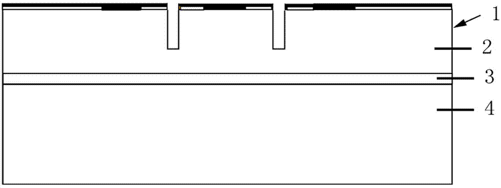
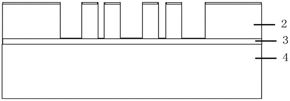
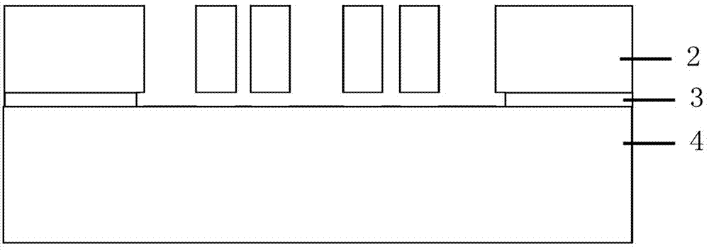
[0015] Figure 1-Figure 4 It is a schematic diagram of the process flow of the double-mask SOI MEMS processing method. This processing method uses SOI wafer 1 to manufacture MEMS devices, and adopts double mask technology, which can effectively reduce the Footing effect at the bottom of the silicon structure layer 2 and reduce the gap between the mass block and other structures on the silicon structure layer 2 and the silicon substrate layer 4. the parasitic capacitance between them.

[0016] exist figure 1 Among them, the SOI wafer 1 includes a layer of silicon dioxide (SiO2) layer 3 located between the silicon structure layer 2 and the silicon substrate layer 4. The silicon structure layer 2 is doped with concentrated boron, and the doping concentration is greater than . The processing method is realized through the following process steps:

[0017] (1) Sputter a layer of aluminum on the front of the silicon wafer, photolithography, etch the aluminum, and define a comp...


PUM


Abstract

The invention provides a processing method for a double-mask silicon on insulator (SOI) micro electro mechanical system (MEMS), which belongs to the field of MEMS micro-processing. An SOI wafer comprises a silicon structural layer, a silicon substrate layer and an insulation layer arranged between the silicon structural layer and the silicon substrate layer. Heavy boron doping is conducted on the silicon structural layer of an SOI wafer sheet, and doping concentration is larger than 5*1018 / cm3. The method includes sputtering a layer of aluminum on the front of a silicon sheet, photoetching, etching aluminum, and defining a complete MEMS structural image on the silicon sheet; photoetching and forming a thin line width structure image on the silicon sheet; etching a thin line width structure by using an inductively coupled plasma (ICP) etching method; removing photoetching glue, and using the ICP etching method for etching the wide thin line width structure simultaneously; etching the insulation layer below the structural layer; and using a KOH solution corrosion method to etch a silicon substrate. The processing method can use an SOI material to manufacture various MEMS devices and has the advantages of being good in controllability of structural layer thickness, reducing footing effect and parasitic capacitance, being simple in processing flow and the like.

Description

technical field [0001] The present invention relates to the micro-machining technical field of micro-electromechanical systems, in particular to a micro-machining process research on a double-mask silicon on insulator (Silicon on insulator, SOI) micro-electromechanical systems (Micro-electromechanical Systems, MEMS) processing method. Background technique [0002] In recent years, SOI technology has made great progress, and its application in the MEMS field has the following advantages: the monocrystalline silicon structure layer has excellent mechanical properties; the SiO2 buried oxide layer as a sacrificial layer and insulating layer has excellent corrosion stop capability, In MEMS processing, it is easy to obtain a complete, defect-free, uniform thickness and precisely controlled structural layer; the thickness of the structural layer can be increased; the all-silicon structure is compatible with the CMOS process and can be integrated with denser circuits. Therefore, com...

Claims


Application Information

Patent Timeline
Patent Type & Authority Patents(China)
IPC IPC(8): B81C1/00
Inventor 张照云高杨彭勃施志贵苏伟
Owner INST OF ELECTRONICS ENG CHINA ACAD OF ENG PHYSICS
Why Eureka
Try Eureka