
Laser diode packaging module and packaging method

A technology for packaging modules and semiconductors, applied to the structural details of semiconductor lasers, etc., can solve the problems of chip and heat dissipation substrate voids, device reliability, and service life, etc., to achieve high photoelectric conversion efficiency, performance and reliability Improvement , the effect of saving time

Inactive Publication Date: 2012-06-20
TIANJIN UNIV
View PDF1 Cites 4 Cited by
  • Summary
  • Abstract
  • Description
  • Claims
  • Application Information

AI Technical Summary

Problems solved by technology

However, the traditional single-tube semiconductor laser packaging method has some shortcomings.
First of all, since the solder used to package single-tube semiconductor lasers in the market currently uses indium and gold-tin solder as chip connection materials, it takes a lot of time to plate solder on the surface of the heat sink; secondly, indium solder and gold-tin solder package single-tube semiconductor lasers. There are some issues with lasers
Indium solder: 1. The solder itself is easy to oxidize; 2. Electromigration of indium will occur under high current; 3. Electrothermal migration is easy to occur at high temperature gradients, which leads to voids between the chip and the heat dissipation substrate
Gold-tin solder: 1. The thermal expansion coefficient of the copper heat sink and GaAs-based LD chip does not match, and other materials need to be used as a cushion to adjust the thermal expansion coefficient; 2. Semiconductor lasers packaged with gold-tin solder, due to the use of cushion materials , the heat dissipation is not good, the thermal resistance is large, and the service life is affected
The preparation of semiconductor lasers needs to ensure their reliability and service life. The use of traditional packaging materials and packaging methods has a certain impact on the reliability of the device itself.

Method used


Image

  • Laser diode packaging module and packaging method
  • Laser diode packaging module and packaging method
  • Laser diode packaging module and packaging method

Examples


Embodiment Construction

[0020] The process of the present invention will be described in detail below in conjunction with the single-tube semiconductor laser module shown in the accompanying drawings.

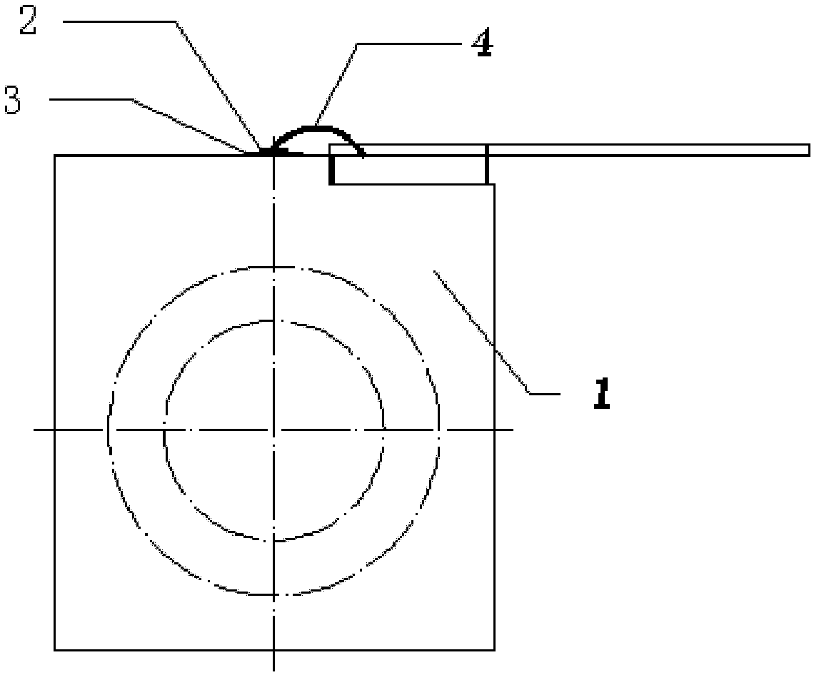
[0021] The packaging module of the single-tube semiconductor laser of the present invention, as shown in FIG. A copper block with good thermal conductivity is selected as the base material of the heat sink 1, and the surface is plated with Ni and Au (the thickness is about 2 μm). The LD chip 2 is based on GaAs and has a size of 0.5mm×2mm. The chip connecting material 3 is nano-silver solder paste with good thermal conductivity, which can ensure good heat dissipation of the chip. This module uses nano-silver solder paste 3 as the connection material of LD chip 2, packages LD chip 2 on heat sink 1, and uses bonding gold wire 4 to connect the negative electrode of LD chip 2 and heat sink 1, and connects the power supply to realize normal operation .

[0022] The single-tube semiconductor laser module ...


PUM

PropertyMeasurementUnit
Thicknessaaaaaaaaaa

Abstract

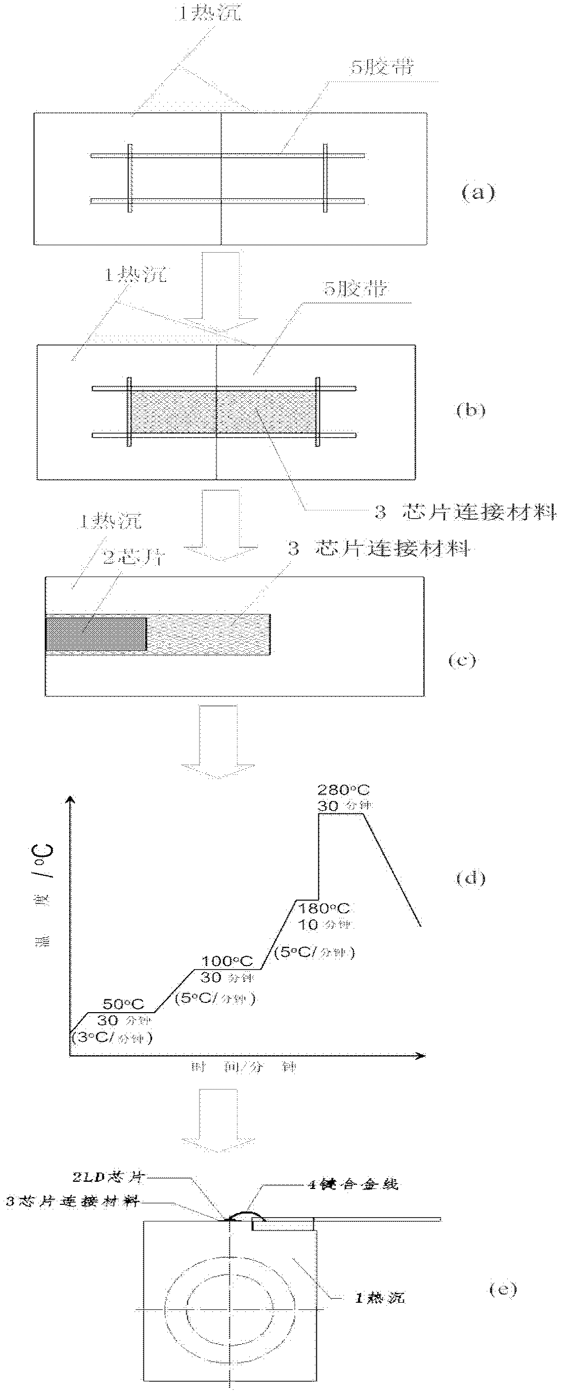
The invention discloses a laser diode (LD) packaging module and a LD packaging method. An LD chip is packaged on a heat sink, nano-silver paste is adopted as a connecting material for the heat sink and the LD chip, and the heat sink is connected with the LD chip through a bonded gold wire to form a negative electrode. In a packaging process, a silk screen printing mold is simulated by an adhesive tape, so that the coating area and thickness of the nano-silver paste are controlled by controlling the arrangement range and thickness of the adhesive tape. The LD chip is connected by a low-temperature sintering technology, and the nano-silver paste is adopted as the connecting material for the LD chip, so that a film can be conveniently plated by a silk screen printing method, film plating time can be effectively saved, and the thickness of the film can be controlled. The connecting material for the LD chip is pure silver, so that the LD packaging module has low thermal resistance, a high integration degree and high photoelectric conversion efficiency, and is energy-saving and environment-friendly.

Description

technical field [0001] The invention relates to a packaging module of a single-tube semiconductor laser (LD) and a packaging method thereof, belonging to the improvement technology of semiconductor laser devices. Background technique [0002] At present, the module for a single-tube semiconductor laser is mainly composed of these parts: heat sink, LD chip packaged on the heat sink, chip connection material, and bonding gold wire connecting the LD chip and the negative electrode of the heat sink. However, the traditional single-tube semiconductor laser packaging method has some shortcomings. First of all, since the solder used to package single-tube semiconductor lasers in the market currently uses indium and gold-tin solder as chip connection materials, it takes a lot of time to plate solder on the surface of the heat sink; secondly, indium solder and gold-tin solder package single-tube semiconductor lasers. There are some problems with lasers. Indium solder: 1. The solder...

Claims


Application Information

Patent Timeline
IPC IPC(8): H01S5/02
Inventor 陈旭鄢艺
Owner TIANJIN UNIV
Learn More