Structure of silicon-substrate GaN-based light-emitting diode (LED) and manufacturing method for silicon-substrate GaN-based LED
A LED structure and LED device technology, applied in electrical components, circuits, semiconductor devices, etc., can solve the problems of sapphire substrate processing difficulty, high cost, total reflection effect of GaN material and air interface and deterioration of LED light-emitting characteristics, etc., to achieve Good electrical and thermal conductivity, good processing characteristics, and good uniformity of white light
- Summary
- Abstract
- Description
- Claims
- Application Information
AI Technical Summary
Problems solved by technology
Method used
Image


Examples
Embodiment 1
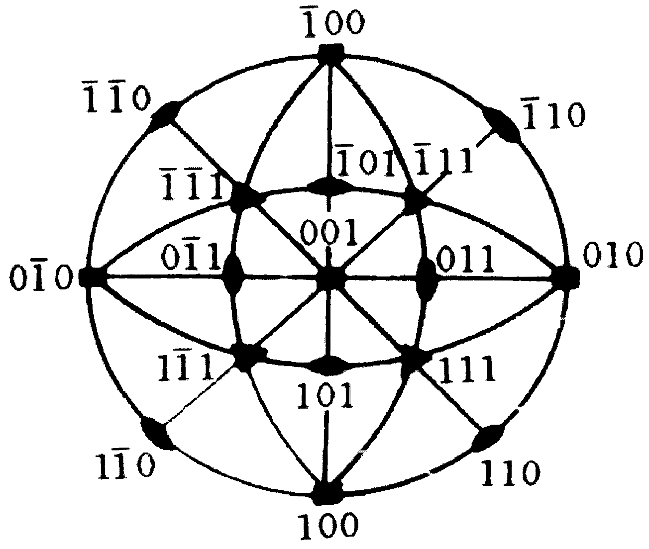
[0076] like figure 2 As shown, the surface of the Si substrate is the (100) crystal plane of Si, that is, the non-(111) crystal plane is the (100) crystal plane. Wherein the Si substrate may be insulating or highly doped conductive Si.
[0077] A mask is made on the (100) crystal plane 1 of the Si substrate, and the mask can be a strip mask, a rectangle, a parallelogram, or a square mask. In the first embodiment disclosed by the present invention is used as Figure 4 For the strip mask 8 shown, the width of the strip mask 8 is 20 microns, the mask pitch is 20 microns, and the side length direction of the strip mask is parallel to the crystal orientation of the Si substrate. It should be noted that the present invention is not limited to the width and pitch of the mask.
[0078] Based on the strip mask 8, the (111) system crystal plane 2 of the Si substrate is corroded and exposed by using an etching solution that has a selective etching effect on the (111) system c...
Embodiment 2
[0095] like Figure 7 As shown, the surface of the Si substrate is the (110) crystal plane of Si, that is, the non-(111) crystal plane is the (110) crystal plane 11 . Wherein the Si substrate may be insulating or highly doped conductive Si.
[0096] A mask is made on the (110) crystal plane 11 of the Si substrate, and the mask can be a strip mask, a rectangle, a parallelogram, or a square mask. In the second embodiment disclosed by the present invention is used as Figure 4 As shown in the strip mask 8, the width of the strip mask 8 is 20 microns, the mask pitch is 20 microns, and the side length direction of the strip mask 8 is parallel to the system crystal direction of the Si substrate . It should be noted that the present invention is not limited to the width and pitch of the mask.
[0097] Based on the strip mask 8, the (111) system crystal plane 2 of the Si substrate is etched and exposed by using an etching solution that has a selective etching effect on th...
Embodiment 3
[0106] On the basis of the embodiments disclosed in the present invention above, as Figure 9 As shown, the surface of the Si substrate is the (100) crystal plane 1 of Si, and a mask is carried out on the (100) crystal plane 1 of the Si substrate. The mask is as follows Figure 8 As shown in the square mask 12, the width of the square mask 12 is 100 microns, the mask spacing is 440 microns, and the side length direction of the square mask 12 is parallel to the crystal orientation of the Si substrate. It should be noted that the present invention is not limited to the width and pitch of the mask.
[0107] Based on the square mask 12, the (111) system crystal plane 2 of the Si substrate is corroded and exposed by using an etchant that has a selective etching effect on the (111) system crystal plane 2 of Si, and the exposed (111) system crystal plane There are at least two planes 2, and the (111) crystal planes may or may not intersect each other.
[0108] The etching ...
PUM
 Abstract
Description
Claims
Application Information
 - R&D
- Intellectual Property
- Life Sciences
- Materials
- Tech Scout
- Unparalleled Data Quality
- Higher Quality Content
- 60% Fewer Hallucinations
Browse by: Latest US Patents, China's latest patents, Technical Efficacy Thesaurus, Application Domain, Technology Topic, Popular Technical Reports.
© 2025 PatSnap. All rights reserved.Legal|Privacy policy|Modern Slavery Act Transparency Statement|Sitemap|About US| Contact US: help@patsnap.com