Manufacturing method of semiconductor laser
A manufacturing method and laser technology, applied to the structure of optical resonant cavity, etc., can solve the problems of inability to effectively reduce cavity surface absorption and high optical power density of lasers, so as to improve the optical catastrophe damage threshold, reduce light absorption, Effect of Reducing Lasing Threshold Current Density
- Summary
- Abstract
- Description
- Claims
- Application Information
AI Technical Summary
Problems solved by technology
Method used
Image
Examples
Embodiment 1
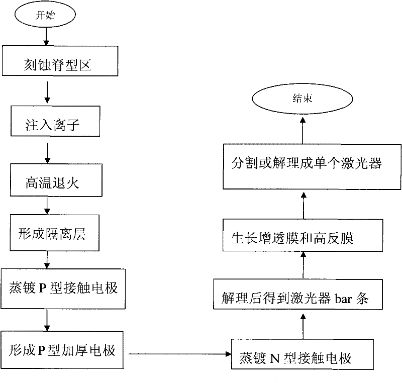
[0034] In this embodiment, a 450nm blue ridge-type GaN-based laser is used. The active region 1 of the laser is an InGaN / GaN multiple quantum well, and the current is injected from the ridge region 2 . Refer to the specific operation flow chart figure 1 , the implementation steps include:
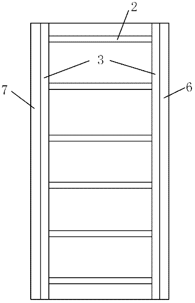
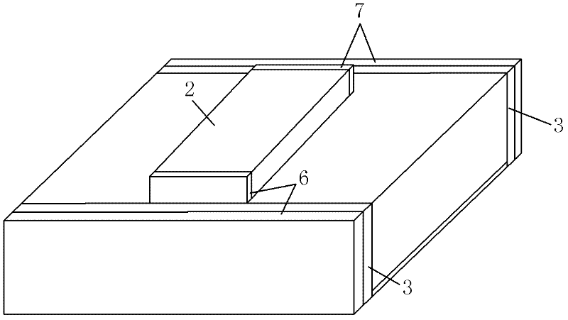
[0035] (1) Using photoetching technology, using photoresist as a mask, using such as figure 2 As shown in the photolithography plate, the ridge region 2 of the laser is etched by ion beams on the laser epitaxial wafer, such as Figure 4 shown. Different lasers have different widths of the ridge-shaped region 2, generally ranging from 1-200 μm, and the width of the ridge-shaped region 2 in this embodiment is 5 μm.
[0036] (2) Using photoetching technology, photoresist is used as a mask near the front and rear cavity surfaces of the laser, and ions are implanted near the front and rear cavity surfaces of the laser from a direction perpendicular to the exit cavity surface of the laser th...
Embodiment 2
[0047] In this embodiment, a 450nm blue ridge-type GaN-based laser is used. The active region 1 of the laser is an InGaN / GaN multiple quantum well, and the current is injected from the ridge region 2 . Refer to the specific operation flow chart figure 1 , the implementation steps include:
[0048] (1) Using photoetching technology, using photoresist as a mask, using such as figure 2 As shown in the photolithography plate, the ridge region 2 of the laser is etched by ion beams on the laser epitaxial wafer, such as Figure 4 shown. Different lasers have different widths of the ridge-shaped region 2, generally ranging from 1-200 μm, and the width of the ridge-shaped region 2 in this embodiment is 5 μm.
[0049] (2) Using photoetching technology, photoresist is used as a mask near the front and rear cavity surfaces of the laser, and ions are implanted near the front and rear cavity surfaces of the laser from a direction perpendicular to the exit cavity surface of the laser th...
Embodiment 3
[0059] In this embodiment, a 450nm blue ridge-type GaN-based laser is used. The active region 1 of the laser is an InGaN / GaN multiple quantum well, and the current is injected from the ridge region 2 . Refer to the specific operation flow chart figure 1 , the implementation steps include:
[0060] (1) Using photoetching technology, using photoresist as a mask, using such as figure 2 As shown in the photolithography plate, the ridge region 2 of the laser is etched by ion beams on the laser epitaxial wafer, such as Figure 4 shown. Different lasers have different widths of the ridge-shaped region 2, generally ranging from 1-200 μm, and the width of the ridge-shaped region 2 in this embodiment is 5 μm.
[0061] (2) Using photoetching technology, photoresist is used as a mask near the front and rear cavity surfaces of the laser, and ions are implanted near the front and rear cavity surfaces of the laser from a direction perpendicular to the exit cavity surface of the laser th...
PUM
 Abstract
Description
Claims
Application Information
 - R&D
- Intellectual Property
- Life Sciences
- Materials
- Tech Scout
- Unparalleled Data Quality
- Higher Quality Content
- 60% Fewer Hallucinations
Browse by: Latest US Patents, China's latest patents, Technical Efficacy Thesaurus, Application Domain, Technology Topic, Popular Technical Reports.
© 2025 PatSnap. All rights reserved.Legal|Privacy policy|Modern Slavery Act Transparency Statement|Sitemap|About US| Contact US: help@patsnap.com


