Preparing method of solar cell slice with pattern
A technology of solar cells and patterns, which is applied in the manufacture of circuits, electrical components, and final products, can solve the problems of single solar products and no personalized design and production, and achieve the expansion of application fields, good energy saving and environmental protection benefits, and tight integration Effect
- Summary
- Abstract
- Description
- Claims
- Application Information
AI Technical Summary
Problems solved by technology
Method used
Image
Examples
Embodiment 1
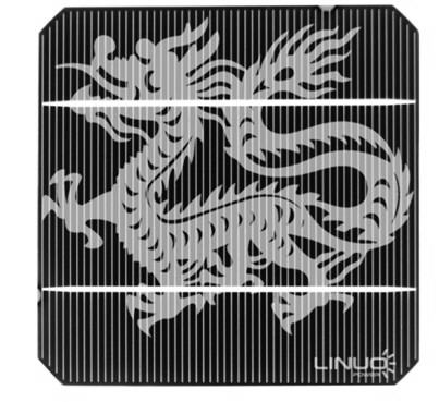
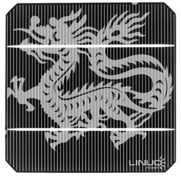
[0026] Example 1: Preparation of 125 single crystal solar cells with dragon pattern
[0027] Select 125 single crystal silicon wafers, the silicon wafers undergo conventional cleaning process, and the surface is textured in order to remove the mechanical damage layer on the surface of the silicon wafer, remove the surface oil and metal impurities, form an uneven textured surface, increase the short-circuit current, and improve the battery life. Photoelectric conversion efficiency. At 260°C, 80-100nm silicon nitride was deposited on the diffusion surface of the silicon wafer by PECVD process (that is, plasma enhanced chemical vapor deposition method). Use a screen with a dragon-shaped pattern to print the Merck acidic corrosive paste on the anti-reflection layer of the silicon wafer by screen printing, place the silicon wafer in an environment of 400°C, and react for 300s. The patterned silicon wafer after the reaction is sprayed with pure water, ultrasonically cleaned, ultras...
Embodiment 2
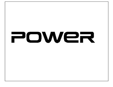
[0029] Embodiment 2: the preparation of 156 polycrystalline solar cells with the words "POWER"
[0030] Select polycrystalline silicon wafers, and the silicon wafers undergo a conventional cleaning process, and the surface is textured to remove the mechanical damage layer on the surface of the silicon wafer, remove surface oil and metal impurities, form an uneven textured surface, increase the short-circuit current, and improve the photoelectric conversion efficiency of the battery . At 260°C, use the PECVD process (that is, plasma enhanced chemical vapor deposition method) to deposit an anti-reflection layer of 80~100nm on the diffusion surface of the silicon wafer. Use a screen with the word "POWER" to print Merck's alkaline corrosive paste on the silicon wafer by screen printing, place the silicon wafer at 150°C, and react for 20 seconds. The patterned silicon wafer is sprayed with pure water, ultrasonically cleaned, ultrasonically cleaned in dilute hydrochloric acid solut...
PUM
 Abstract
Description
Claims
Application Information
 - R&D Engineer
- R&D Manager
- IP Professional
- Industry Leading Data Capabilities
- Powerful AI technology
- Patent DNA Extraction
Browse by: Latest US Patents, China's latest patents, Technical Efficacy Thesaurus, Application Domain, Technology Topic, Popular Technical Reports.
© 2024 PatSnap. All rights reserved.Legal|Privacy policy|Modern Slavery Act Transparency Statement|Sitemap|About US| Contact US: help@patsnap.com


