Structural design for improving power tolerance of micro low-capacitance protective device

A technology for structural design and capacitors, applied in the direction of electrical components, semiconductor/solid-state device manufacturing, circuits, etc., can solve problems such as damage, and achieve the effect of increasing the chip source area, solving process incompatibility, and increasing the area

Inactive Publication Date: 2011-06-29
淮永进 +1
View PDF0 Cites 2 Cited by
  • Summary
  • Abstract
  • Description
  • Claims
  • Application Information

AI Technical Summary

Problems solved by technology

And when the size of electronic equipment is getting smaller and smaller, the functions are more and more, the circuit is more and more sophisticated, and the semiconductor technology used is below sub-micron, the IC design is more sensitive to ESD, and it is more vulnerable to ESD damage, ESD At the same time, low capacitance becomes a design challenge

Method used


Image

  • Structural design for improving power tolerance of micro low-capacitance protective device
  • Structural design for improving power tolerance of micro low-capacitance protective device
  • Structural design for improving power tolerance of micro low-capacitance protective device

Examples


Embodiment Construction

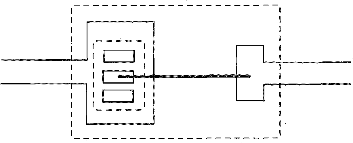
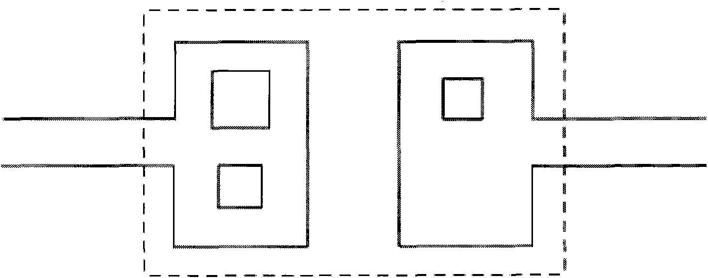
[0011] 1. Weld (conductive glue or eutectic welding) two independent chips on the metal lead frame 1, and then weld a chip on the other end 2 of the metal lead frame to form a one-way device, or weld two chips to form a two-way device.

[0012] 2. After the chip soldering is completed, it must be checked to ensure that the bonding effect of the chip is good, and then wire bonding is performed as shown in Figure 3, and finally plastic packaging is performed to form an independent device.

[0013] The invention of "a structural design for improving the power tolerance of miniature low-capacitance protection devices" lies in:

[0014] 1 Multi-core assembly, anti-power, low capacitance.

[0015] 2 Micro package, the overall size is less than or equal to 1.2mm*1mm*0.5mm.

[0016] 3 Dual carriers carry multiple chips.

[0017] Advantages of "a structural design to improve the power tolerance of miniature low-capacitance devices":

[0018] 1 The chip production process is simple. ...


PUM


Abstract

With the continual increase of the transfer speed of communication equipment, a data line protective device has lower and lower capacitance, but the power tolerance is still higher, so that the traditional machined structure can not meet the design requirements. Although the integration of a transient voltage suppressor (TVS) chip and a low-capacitance device chip on the same chip can reduce the occupied space of the chip, the power tolerance can incur loss accordingly. The invention relates to a structural design for improving the power tolerance of a micro low-capacitance protective device. A group of TVS chips and the low-capacitance device are independently designed, and are encapsulated in a structure disclosed in the drawing, thereby greatly lowering the chip machining difficulty and properly increasing the TVS area. The TVS chips and the low-capacitance device can be assembled in the same micro encapsulation body, thus the conflict between low capacitance and high power is solved.

Description

technical field [0001] The invention belongs to the field of microelectronic devices, and rationally arranges multiple chips in a plastic package with a very small space, thereby solving the contradiction between miniaturization and power tolerance. [0002] Its multi-chip packaging not only solves the processing difficulty of the chip, but also greatly increases the source area of ​​the anti-power chip, completely solves the process incompatibility between low-capacitance devices and power devices, greatly increases the power tolerance, and greatly reduces the value of low-capacitance . Background technique [0003] In the past, ESD did not seem to be a problem because electronic equipment was not so small and the IC devices used were much larger than they are now. Because larger devices also have higher capacitance, they can hold more charge per volt (V) and are therefore less susceptible to ESD than smaller devices. And when the size of electronic equipment is getting s...

Claims


Application Information

Patent Timeline
IPC IPC(8): H01L21/50H01L21/58H01L21/60
Inventor 淮永进
Owner 淮永进
Why Eureka
Try Eureka