
Receiving module package method for optical interconnection on chip

A receiving module and packaging method technology, applied in the direction of optical waveguide light guide, electrical components, circuits, etc., can solve the problems of low integration, high cost, and inability to use chips for shorter distance communication

Inactive Publication Date: 2011-04-06
INST OF SEMICONDUCTORS - CHINESE ACAD OF SCI
View PDF0 Cites 13 Cited by
  • Summary
  • Abstract
  • Description
  • Claims
  • Application Information

AI Technical Summary

Problems solved by technology

[0003] At present, most optical interconnection technologies mainly use optical fiber as the transmission medium. The transceiver module and the receiving module are packaged chips. The interconnection system faces problems such as large volume, low integration, and high cost, so it can only be applied to boards and Long-distance interconnection between boards cannot be applied to shorter-distance communication between different chips on the same board

Method used


Image

  • Receiving module package method for optical interconnection on chip
  • Receiving module package method for optical interconnection on chip
  • Receiving module package method for optical interconnection on chip

Examples


Embodiment Construction

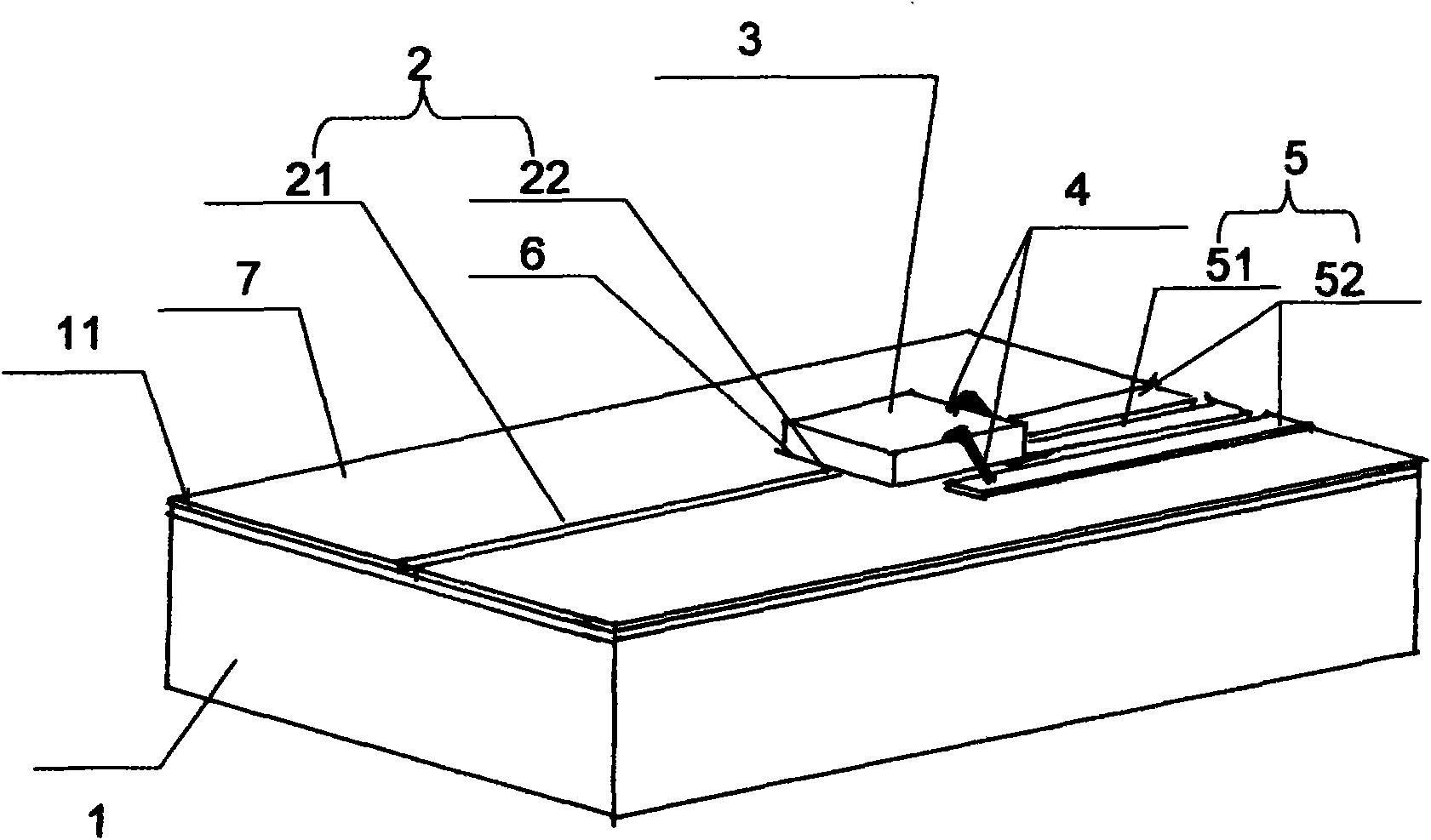
[0025] see figure 1 , a receiving module packaging method for on-chip optical interconnection, the method includes the following manufacturing steps:

[0026] Step 1: First, clean the SOI substrate 1 to remove organic and inorganic impurities on the substrate, and then evenly coat the electron beam photoresist on the surface of the SOI substrate 1 through a coater. Based on methyl acrylate glue (PMMA) photoresist, pre-baking the SOI substrate 1 after coating, the pre-baking temperature is 180 degrees Celsius, and the time is 20 minutes, and then put the SOI substrate 1 into the electron beam exposure machine, Select an appropriate exposure dose to expose the pattern of the grating coupler 2 including the ridge waveguide 21 and the grating structure 22, then develop and fix, and finally perform post-baking on the exposed SOI substrate 1 at a post-baking temperature of 120 degrees Celsius , and the time is 20 minutes. After electron beam exposure, a fine submicron pattern is fo...


PUM

PropertyMeasurementUnit
Lengthaaaaaaaaaa
Etching depthaaaaaaaaaa
Thicknessaaaaaaaaaa

Abstract

The invention discloses a receiving module package method for optical interconnection on a chip, comprising the following steps of: transferring a ridge waveguide and a grating structure on a domain to a top silicon layer on an SOI (Silicon On Insulator) chip cleaned in advance by adopting an electron beam exposure technology; with electron beam resist as a mask, etching a submicron ridge waveguide and a grating structure by using a silicon plasma dry-method etching process; covering a silicon dioxide insulating layer on the surface of the etched graph by adopting a silicon dioxide precipitating technology; transferring a metal lead and an aligning mark graph to the silicon dioxide insulating layer by adopting a general photoetching method; producing the metal lead and an aligning mark by using a metal evaporation process; accurately backing off a photoelectric detector to the preset position on the SOI chip by using the aligning mark on the SOI chip and a flip chip bonding technology; connecting the grounded surface on the back of the photoelectric detector with a grounded wire on the SOI chip by using an interconnected gold wire; and filling setting glue between the photoelectric detector and the SOI chip for curing and sealing to finish the package of the device.

Description

technical field [0001] The invention belongs to the technical field of semiconductor optoelectronics, in particular to a receiving module packaging method for on-chip optical interconnection. Background technique [0002] The continuous advancement of information technology has made the feature size of semiconductor chips smaller and smaller, the number of transistors is increasing, and the processing speed of chips is getting faster and faster. The problems caused by the interconnection of chips with metal wires (transmission delay, Signal crosstalk, etc.) is becoming more and more serious, especially in the bus system between chips, the amount of data that needs to be transmitted and exchanged is large, and the transmission distance is long, so the problems caused by electrical interconnection are more serious. Optical interconnection is a technology that utilizes the characteristics of light waves and their interaction with optical materials to realize data and signal tra...

Claims


Application Information

Patent Timeline
IPC IPC(8): H01L31/18G02B6/13
Inventor 徐海华肖希朱宇李运涛俞育德余金中
Owner INST OF SEMICONDUCTORS - CHINESE ACAD OF SCI
Learn More