
Preparation method of Cu2ZnSnS4 photovoltaic film

A photovoltaic thin film and thin film technology, applied in the direction of final product manufacturing, sustainable manufacturing/processing, ion implantation plating, etc., can solve the problems of difficult to obtain practical application, poor uniformity over large areas, poor reproducibility, etc. The effect of large-scale promotion, improved phase crystallization quality, and simple process

Inactive Publication Date: 2011-02-09
CENT SOUTH UNIV
View PDF0 Cites 5 Cited by
  • Summary
  • Abstract
  • Description
  • Claims
  • Application Information

AI Technical Summary

Problems solved by technology

Among them, the quality of the film prepared by evaporation is high, but the biggest development bottleneck of this technology is the poor uniformity of large area, which makes it difficult to obtain practical application
After the prefabricated layer is vulcanized, the alloy prefabricated layer is first prepared by sputtering, electroplating, etc., and then the prefabricated layer is heat treated (sulfurized) to obtain Cu 2 ZnSnS 4 Thin film, this method is easy to achieve large-area preparation of thin film, but there are problems such as complex process, long process, and poor reproducibility

Method used

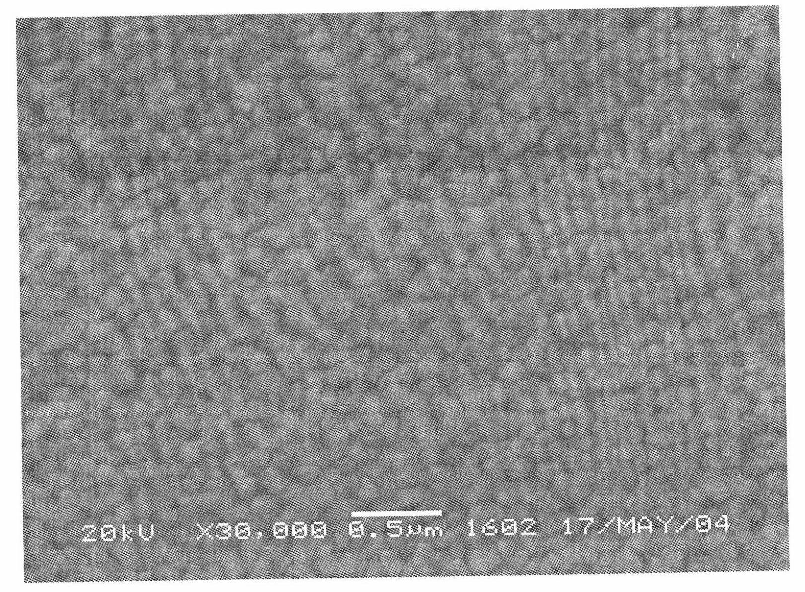
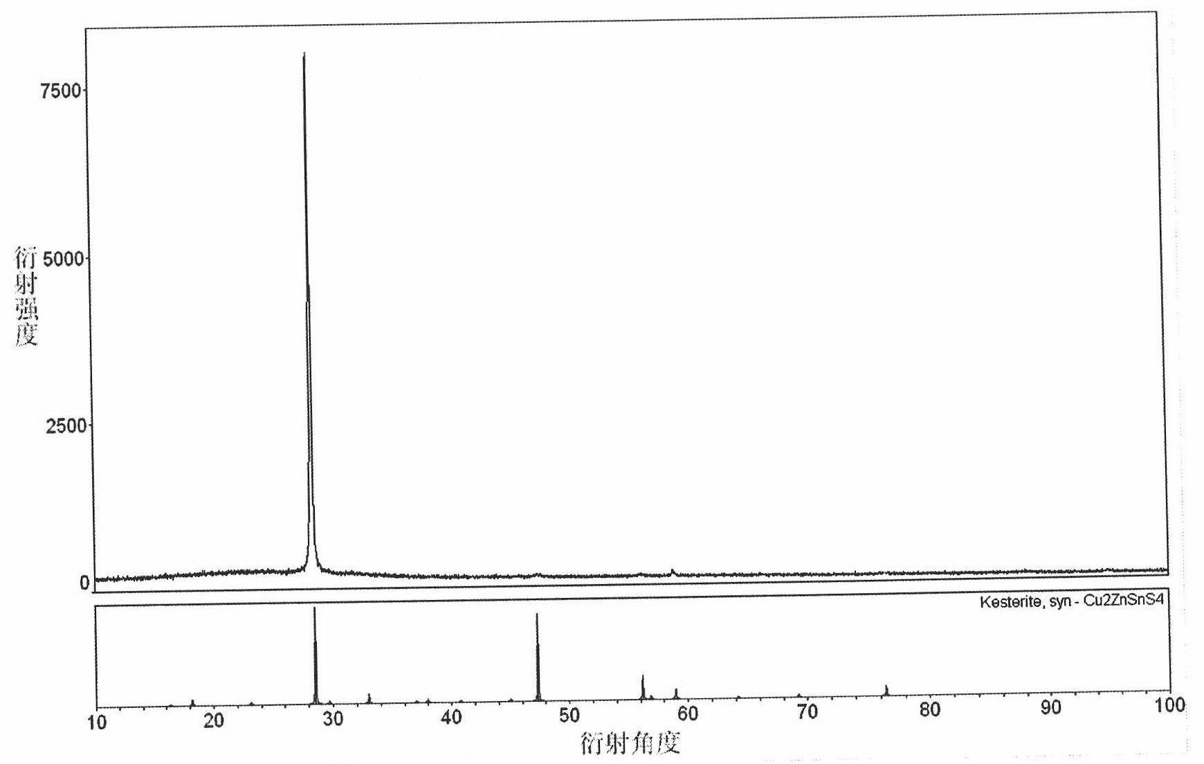
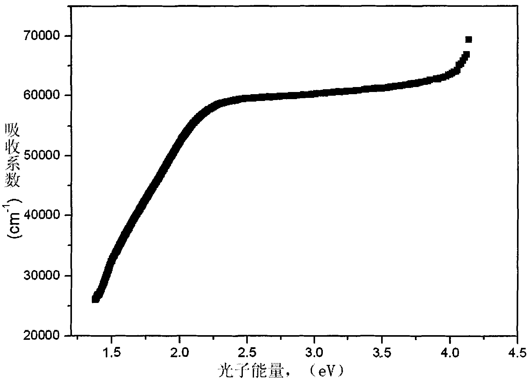

Image

  • Preparation method of Cu2ZnSnS4 photovoltaic film
  • Preparation method of Cu2ZnSnS4 photovoltaic film
  • Preparation method of Cu2ZnSnS4 photovoltaic film

Examples


Embodiment 1

[0017] The Cu-Zn-Sn alloy target with an atomic ratio of Cu:Zn:Sn=1:0.2:1.7 is used as the cathode target, and the DC sputtering method is adopted, and the sputtering power is 160W; the mixed gas of hydrogen sulfide and argon is used as the sputtering Sputtering gas, the volume fraction of hydrogen sulfide in the mixed gas is 5%; the sputtering pressure is 0.08Pa, the distance between the target and the substrate is 8cm, the substrate temperature is 350°C, and the speed is rotated at 100 rpm. thin film deposition. Obtain Cu with a thickness of 1.2 μm 2 ZnSnS 4 Photovoltaic thin film, its conductivity type is p-type, and its bandgap width is 1.51eV.

Embodiment 2

[0019] The Cu-Zn-Sn alloy target with an atomic ratio of Cu:Zn:Sn=1:0.5:0.5 is used as the cathode target, and the DC sputtering method is adopted, and the sputtering power is 80W; the mixed gas of hydrogen sulfide and argon is used as the sputtering Sputtering gas, the volume fraction of hydrogen sulfide in the mixed gas is 80%, the sputtering pressure is 1Pa, the distance between the target and the substrate is 11cm, the substrate temperature is 500°C, and rotates at a rate of 4 revolutions per minute to perform thin film deposition. Obtain Cu with a thickness of 1 μm 2 ZnSnS 4 Photovoltaic thin film, its photoelectricity and other performance parameters are as follows:

[0020] thickness

Embodiment 3

[0022] The Cu-Zn-Sn alloy target with an atomic ratio of Cu:Zn:Sn=1:1.7:0.3 is used as the cathode target, and the radio frequency sputtering method is adopted, and the sputtering power is 30W; the hydrogen sulfide gas is used as the sputtering gas, and the sputtering The air pressure is 5Pa, the distance between the target and the substrate is 6cm, the substrate temperature is 650°C, and the thin film is deposited without rotation. Obtain Cu with a thickness of 0.5 μm 2 ZnSnS 4 Photovoltaic thin film, its conductivity type is p-type, and its bandgap width is 1.48eV.


PUM

PropertyMeasurementUnit
thicknessaaaaaaaaaa
thicknessaaaaaaaaaa

Abstract

The patent refers to the field of 'coating metallic material; coating material with metallic material; surface treatment of metallic material by diffusion into the surface, by chemical conversion or substitution; coating by vacuum evaporation, by sputtering, by ion implantation or by chemi'. The invention relates to a preparation method of a Cu2ZnSnS4 photovoltaic film, which is characterized by comprising the following step of: depositing a film in a magnetron reactive sputtering way by taking a mixed gas of hydrogen sulfide and argon as a sputtering gas and a Cu-Zn-Sn alloy target as a cathode target, wherein the alloy target comprises the following components with the atomic ratio of Cu:Zn:Sn=1:0.1-2:0.1-2, pressure intensity inside a sputtering chamber during sputtering is 0.05-10 Pa, the distance between the alloy target and a substrate is 3-15 cm, the sputtering power of the cathode target is 15-300 W, the temperature of the substrate is 20-700 DEG C, the substrate rotates at the speed of 0-1000 turns / minute, and the thickness of the grown film is 0.2-5 micrometers. Compared with the traditional technology based on thermal activation, the Cu2ZnSnS4 photovoltaic film prepared by the method has good large-area component uniformity, high crystallization quality and few impure phase; in addition, the method also has the advantages of simple process, low cost, good repeatability, and the like.

Description

technical field [0001] The invention belongs to the technical field of new energy sources of photoelectric materials, and relates to a growth method of a compound semiconductor thin film used as a light absorption layer of a thin film solar cell. Background technique [0002] The development of solar cells is an effective way to solve the worsening energy crisis and environmental pollution. Among all kinds of solar cells, CuIn 1-x Ga x Se 2 (CIGS) thin-film solar cells are considered to be one of the most important and most promising solar cells due to their excellent photovoltaic properties. However, CuIn 1-x Ga x Se 2 In, Ga, and Se in the compound are scattered metals, which are expensive and have limited reserves. Therefore, it is necessary to search for high-abundance elements and low-cost light-absorbing layer film materials to replace CuIn 1-x Ga x Se 2 has become an important topic before us. It must be pointed out that in order to realize the large-scale ...

Claims


Application Information

Patent Timeline
Patent Type & Authority Applications(China)
IPC IPC(8): C23C14/06C23C14/35H01L31/18
CPCY02P70/50
Inventor 刘芳洋赖延清张坤李轶张治安匡三双李劼刘业翔
Owner CENT SOUTH UNIV
Learn More