Single nanowire electrochemical device and assembly and in-situ characterization method thereof
A rice wire and nanowire technology, applied in the field of in-situ characterization, single nanowire electrochemical devices and their assembly
- Summary
- Abstract
- Description
- Claims
- Application Information
AI Technical Summary
Problems solved by technology
Method used
Image
Examples
Embodiment 1
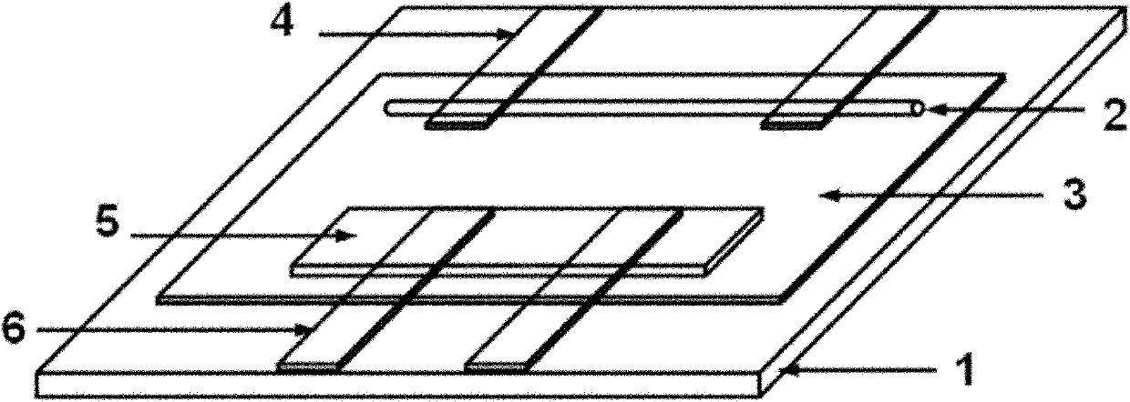
[0025] The technical solution for the assembly of a single nanowire electrochemical device includes the following steps, which are carried out in sequence:
[0026] 1) V prepared by hydrothermal method 3 o 7 ·H 2 O nanowire positive electrode and highly ordered pyrolytic graphite flake film negative electrode are dispersed on the surface with a layer of 60 nm thick SiO 2 on the silicon substrate; where, V 3 o 7 ·H 2 The preparation method of O nanowires can refer to the following documents: H, Qiao, et al.Electrochem.Commun.8, 21-26 (2006); Y.Oka, et al.J.Solid State Chem.89, 372-377 ( 1990); high-order pyrolytic graphite flake film is prepared by tearing tape method, can refer to the following literature K.S.Novoselov, et al.Science, 306, 666-669 (2004);
[0027] 2) making Cr (5nm) and Au (80nm) metal electrodes as current collectors at the two ends of the nanowire and the nanofilm respectively by electron beam lithography;
[0028] 3) Using PECVD technology to deposit...
Embodiment 2
[0034] The technical scheme adopted for the assembly of a single nanowire electrochemical device includes the following steps, which are carried out in sequence:
[0035] 1) The coaxial Si / a-Si nanowire anode and LiCoO 2 The thin-film positive electrode is dispersed and deposited on the surface with a layer of 60nm thick SiO 2 on a silicon substrate; wherein, coaxial Si / a-Si nanowires are prepared by chemical vapor deposition, and the preparation method refers to the following literature: L.F.Cui, et al.Nano Lett., 9, 491-495(2009); LiCoO 2 The film was prepared by magnetron sputtering, and the film deposition conditions were: deposition for 10 minutes, annealing at 500°C for 2.5 hours;
[0036] 2) Electron beam lithography is used to fabricate Cr (5nm) and Au (80nm) metal electrodes at both ends of the nanowire and the nanofilm as current collectors;
[0037] 3) Using PECVD technology to deposit 500nm thick silicon nitride on the metal current collector as a protective laye...
Embodiment 3
[0043] The technical scheme adopted for the assembly of a single nanowire electrochemical device includes the following steps, which are carried out in sequence:
[0044] 1) β-AgVO 3 The positive electrode of nanowires and the negative electrode of highly ordered pyrolytic graphite flake film are dispersed on the substrate of polydimethylsiloxane (PDMS) insulation; among them, β-AgVO 3 The nanowires are prepared by a hydrothermal method, and reference can be made to the following literature: L.Q.Mai, et al.Nano Lett., 10, 2604-2608 (2010); the preparation method of the high-order pyrolytic graphite sheet is the same as that of Example 1;
[0045] 2) Ti (5nm) and Al (80nm) metal electrodes are fabricated as current collectors at both ends of the nanowire and the nanofilm by electron beam lithography;
[0046] 3) Prepare a 500nm thick SU8 photoresist on the metal current collector by photolithography technology as the protective layer of the current collector;
[0047] 4) LiBF...
PUM
 Abstract
Description
Claims
Application Information
 - R&D
- Intellectual Property
- Life Sciences
- Materials
- Tech Scout
- Unparalleled Data Quality
- Higher Quality Content
- 60% Fewer Hallucinations
Browse by: Latest US Patents, China's latest patents, Technical Efficacy Thesaurus, Application Domain, Technology Topic, Popular Technical Reports.
© 2025 PatSnap. All rights reserved.Legal|Privacy policy|Modern Slavery Act Transparency Statement|Sitemap|About US| Contact US: help@patsnap.com


