Recording element substrate, method of manufacturing the recording element substrate, and liquid ejection head
一种记录元件、基板的技术,应用在印刷等方向,能够解决不能散热、喷墨定时偏移、温度增加等问题,达到可靠性高的效果
- Summary
- Abstract
- Description
- Claims
- Application Information
AI Technical Summary
Problems solved by technology
Method used
Image
Examples
no. 1 example
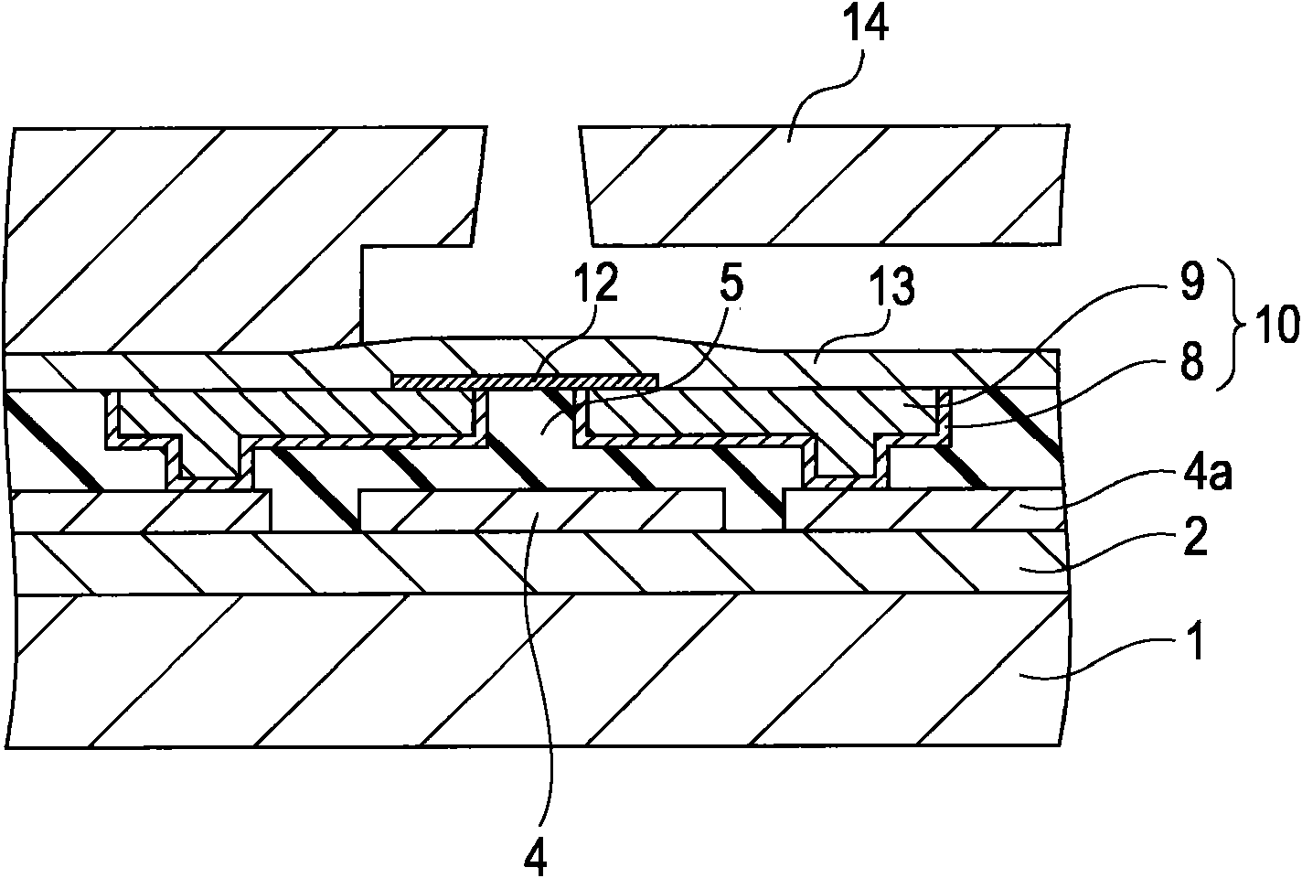
[0039] will refer to figure 2 and image 3 Examples of the present invention will be described. Such as figure 2 As shown, on a Si substrate 1 provided with active elements (active elements) (not shown) such as transistors, SiO doped with boron or phosphorus with a thickness of 500 nm is provided. 2 Formed interlayer film 2. On the interlayer film 2, a heat conduction layer 4 made of an Al-Si alloy and an electrode layer 4a having a thickness of 400 nm are provided. On the thermal conduction layer 4 and the electrode layer 4a, a layer made of SiO with a thickness of 1 μm is set. 2 The insulating layer 5 is formed. The insulating layer 5 also functions as a heat storage layer that stores the heat of the heating portion 12 . A heating portion 12 made of TaSiN with a thickness of 50 nm was provided on the insulating layer 5 . Both ends of each heating unit 12 are in contact with the electrodes 10 . The electrode 10 is in contact with the electrode layer 4 a via a contac...
no. 2 example
[0055] Figure 7A and Figure 7B An example according to the second embodiment of the present invention is shown. Except for the shape of the heat conduction member 11, the structure and manufacturing method of the second embodiment are the same as those of the first embodiment, and therefore, repeated descriptions will be omitted. As shown in the first embodiment, by setting as figure 1 The heat conducting member 11 shown prevents thermal interference. In the case where a higher speed is required, it can be adjusted by increasing the volume of the heating part 12 . However, if the distance between each heat-conducting member 11 and the heating portion 12 adjacent to the heat-conducting member 11 is too small, the insulating layer 5 cannot produce an effect as a heat storage layer, and the heat of the heating portion 12 is lost before the ink undergoes film boiling. The heat escapes to the heat conducting member 11 . Therefore, the heat conduction member 11 must be locat...
no. 3 example
[0058] Figure 8A and Figure 8B An example according to the third embodiment of the present invention is shown. Except for the shape of the heat conduction member 11, the structure and manufacturing method of the third embodiment are the same as those of the first embodiment, and therefore, repeated descriptions will be omitted.
[0059] Figure 8A and Figure 8B is shown as Figure 6 A schematic plan view of an end portion of an arrangement (arrangement) of heating portions 12 arranged at a predetermined pitch is shown. In the recording element substrate 1050, since the heating portions 12 are located at a high density in the central region, heat is stored more easily in the central region than in the end regions. When there is a temperature variation between the central region and the end regions of the recording element substrate 1050, the ink on the heating portion 12 located in the central region is burned faster than the ink on the heating portion 12 located in the...
PUM
 Abstract
Description
Claims
Application Information
 - R&D Engineer
- R&D Manager
- IP Professional
- Industry Leading Data Capabilities
- Powerful AI technology
- Patent DNA Extraction
Browse by: Latest US Patents, China's latest patents, Technical Efficacy Thesaurus, Application Domain, Technology Topic, Popular Technical Reports.
© 2024 PatSnap. All rights reserved.Legal|Privacy policy|Modern Slavery Act Transparency Statement|Sitemap|About US| Contact US: help@patsnap.com


