
Method of producing surface acoustic wave devices by exposing X-rays

A surface acoustic wave device and X-ray technology, applied in the direction of electrical components, impedance networks, etc., can solve the problems of low work efficiency and high cost, achieve the effects of reducing production cost, improving working frequency and performance, and improving production efficiency

Active Publication Date: 2012-05-23
INST OF MICROELECTRONICS CHINESE ACAD OF SCI
View PDF0 Cites 0 Cited by
  • Summary
  • Abstract
  • Description
  • Claims
  • Application Information

AI Technical Summary

Problems solved by technology

Due to the strong backscattering effect of the electrode material on the electron beam, it affects the further reduction of the width and spacing of the IDT electrodes
Another disadvantage of electron beam direct writing lithography is lower work efficiency and higher cost

Method used


Image

  • Method of producing surface acoustic wave devices by exposing X-rays
  • Method of producing surface acoustic wave devices by exposing X-rays
  • Method of producing surface acoustic wave devices by exposing X-rays

Examples


Embodiment Construction

[0045] In order to make the object, technical solution and advantages of the present invention clearer, the present invention will be described in further detail below in conjunction with specific embodiments and with reference to the accompanying drawings.

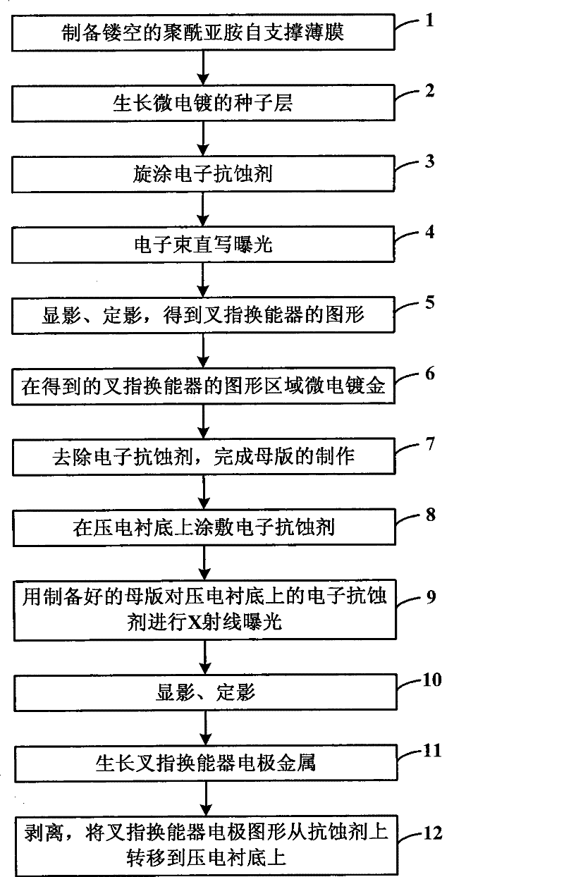
[0046] The invention adopts X-ray photolithography technology, which is an effective nano-processing method and has nano-level resolution. The present invention mainly utilizes electron beam lithography to prepare a master plate for X-ray exposure, and then uses X-ray exposure to form an electronic resist concave vertical electrode pattern of an interdigital transducer with a spacing of less than 500 nm on a piezoelectric substrate, and then grows Surface acoustic wave devices can be prepared by interdigital transducer electrode metal and peeling off.

[0047] Such as figure 1 as shown, figure 1 It is a flowchart of a method for fabricating a surface acoustic wave device by X-ray exposure provided by the present inventi...


PUM


Abstract

The invention discloses a method of producing surface acoustic wave devices by exposing X-rays. A master set of an interdigital transducer is produced by photoetching electron beams on a hollow polyimide self-supporting film; electron beam resist concave solid figures of the interdigital transducer are obtained by exposing X-rays on a piezoelectric substrate; and various surface acoustic wave devices are produced with the stripping technology. By adopting the method of producing the surface acoustic wave devices by exposing X-rays, the back scattering effect of the material of the nano-scale interdigital transducer electrode can be greatly reduced, the nano-scale interdigital transducer electrode can be obtained, and the working performance and the performance of the surface acoustic wavedevices are improved; and in addition, the X-rays can be exposed repeatedly for many times, thus the producing efficiency of the surface acoustic wave devices is improved, and the producing cost is lowered.

Description

technical field [0001] The invention relates to the technical field of micro-nano processing in microelectronics and surface acoustic wave devices, in particular to a method for manufacturing surface acoustic wave devices by X-ray exposure, that is, a method for manufacturing electrodes with nanoscale interdigital transducers. Background technique [0002] According to the transmission properties of surface acoustic waves, for common piezoelectric media, when the working center frequency reaches 1 GHz, the electrode of the interdigital transducer will be smaller than 1 micron. As the operating frequency of the mobile communication system climbs above 2GHz and the development of high-speed sensing technology poses challenges to the manufacture of surface acoustic wave devices, the lines are required to be thinner and the precision higher and higher, even reaching a hundred nanometers or so. Meet the requirements of the rapid development of the mobile communication market and ...

Claims


Application Information

Patent Timeline
Patent Type & Authority Patents(China)
IPC IPC(8): H03H3/08
Inventor 赵以贵李晶晶朱效立牛洁斌刘明
Owner INST OF MICROELECTRONICS CHINESE ACAD OF SCI
Learn More