
Integrated circuit resisting NMOS element total dose radiation

A technology of total dose irradiation and integrated circuits, applied in the field of electronics, can solve the problems of increasing integrated circuit power consumption, large off-state leakage current, etc., achieve reduced off-state leakage current, simple manufacturing process steps, and enhanced anti-total dose radiation The effect of photo performance

Inactive Publication Date: 2010-03-10
PEKING UNIV
View PDF0 Cites 2 Cited by
  • Summary
  • Abstract
  • Description
  • Claims
  • Application Information

AI Technical Summary

Problems solved by technology

Before the device supervisor is turned on, the supervisor is in the off state, but at this time the parasitic tube has been turned on, resulting in a large off-state leakage current
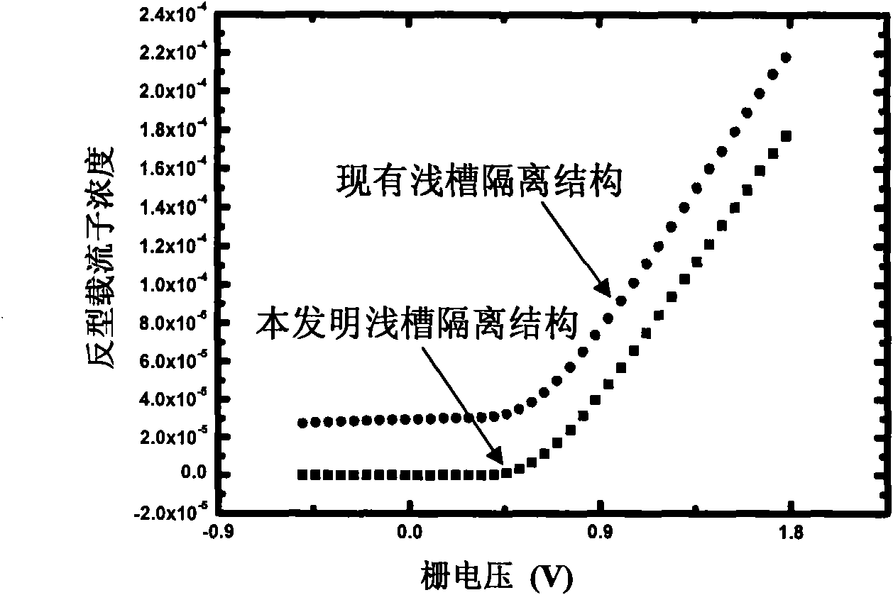
This off-state leakage current will greatly increase the power consumption of the integrated circuit, and have a relatively large negative impact on the reliability of the integrated circuit, which has become a total dose radiation reliability problem that needs to be solved urgently at this stage.

Method used


Image

  • Integrated circuit resisting NMOS element total dose radiation
  • Integrated circuit resisting NMOS element total dose radiation
  • Integrated circuit resisting NMOS element total dose radiation

Examples


Embodiment Construction

[0017] The present invention will be further described below through a specific preparation example in conjunction with the accompanying drawings.

[0018] In this embodiment, the integrated circuit prepared according to the total dose irradiation of NMOS devices according to the present invention mainly includes the following steps:

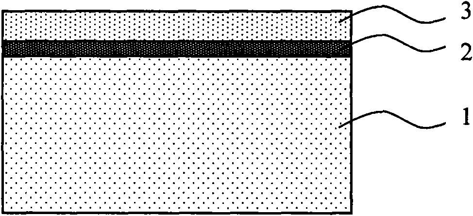
[0019] 1) Formation of silicon dioxide and silicon nitride. like image 3 As shown, a layer of silicon dioxide with a thickness of about 100 angstroms to 200 angstroms is grown by thermal oxidation on a silicon substrate 1 as a stress buffer layer 2 between silicon nitride and the silicon substrate, and then a low-pressure chemical vapor phase is used to Deposition (LPCVD) method deposits a layer of 1000 angstrom to 1500 angstrom silicon nitride as the barrier layer 3 .

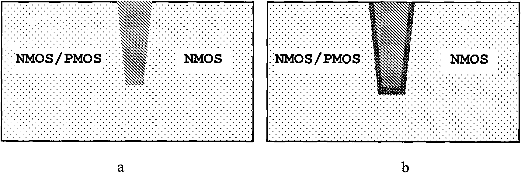
[0020] 2) Trench lithography and etching. like Figure 4 As shown, after defining the shown pattern with photolithography, the trapezoidal trench 4 is etched between the MO...


PUM


Abstract

The invention discloses an integrated circuit resisting NMOS total dose radiation, belonging to the technical field of electronics. The integrated circuit resisting NMOS total dose radiation comprisesan NMOS element and can also comprises a PMOS element, wherein the elements are insulated by a groove on a substrate. The integrated circuit resisting NMOS total dose radiation is characterized in that an insulation material exists between a groove filling material and a substrate material in the groove adjacent to NMOS element and generates fixed negative charges under total dose radiation. Theinsulation material is selected from silicon nitride, titanium nitride and tantalum nitride or a mixture thereof. The thickness of the insulation material ranges from 10 nm to 80 nm. The invention canbe applied to spaceflight, military, nuclear power, high energy physics and other industries relevant to total dose radiation.

Description

technical field [0001] The invention relates to an integrated circuit, in particular to an integrated circuit capable of resisting total dose irradiation of NMOS devices, and belongs to the field of electronic technology. Background technique [0002] Integrated circuit technology is being more and more widely used in industries related to total dose radiation, such as aerospace, military, nuclear power and high-energy physics. Moreover, with the continuous improvement of the integration level of integrated circuits, the size of semiconductor devices is decreasing day by day. Shallow trench isolation technology is becoming the mainstream technology for electrical isolation between devices in integrated circuits due to its excellent device isolation performance. However, due to the damage of the silicon dioxide oxide layer in the device by the total dose of irradiated particles, a large amount of fixed positive charges will be generated in the oxide layer of the shallow trenc...

Claims


Application Information

Patent Timeline
Patent Type & Authority Applications(China)
IPC IPC(8): H01L27/02H01L27/04
Inventor 刘文黄如
Owner PEKING UNIV
Learn More