Soft support cantilever beam type silicon micro-piezoelectric microphone chip and preparation method thereof
A cantilever beam, electro-microphone technology with applications in the fabrication/assembly of piezoelectric/electrostrictive devices, piezoelectric/electrostrictive/magnetostrictive devices, material selection for piezoelectric or electrostrictive devices Equal direction, can solve the problem of low microphone sensitivity
- Summary
- Abstract
- Description
- Claims
- Application Information
AI Technical Summary
Problems solved by technology
Method used
Image
Examples
Embodiment 1
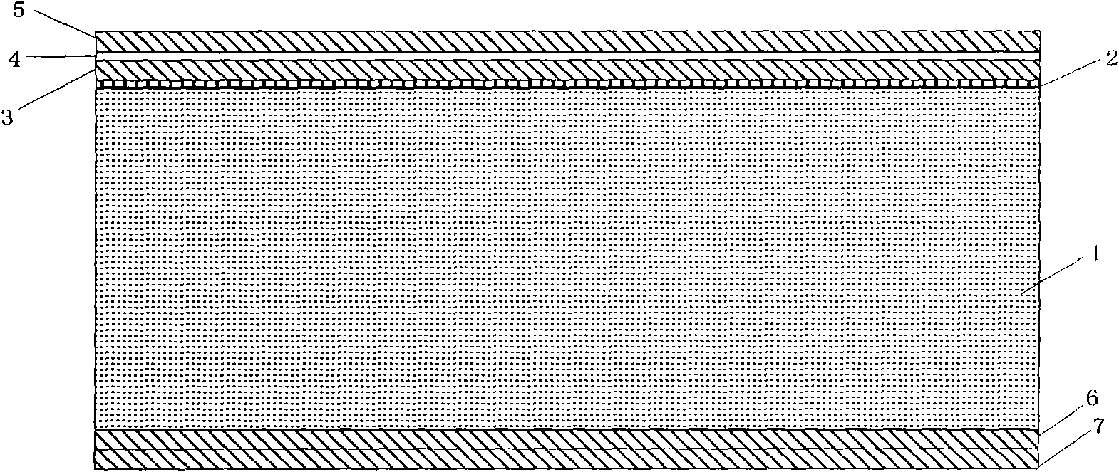
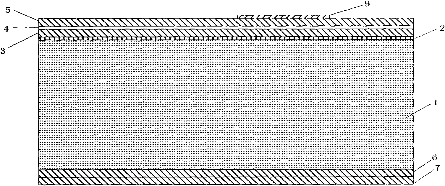
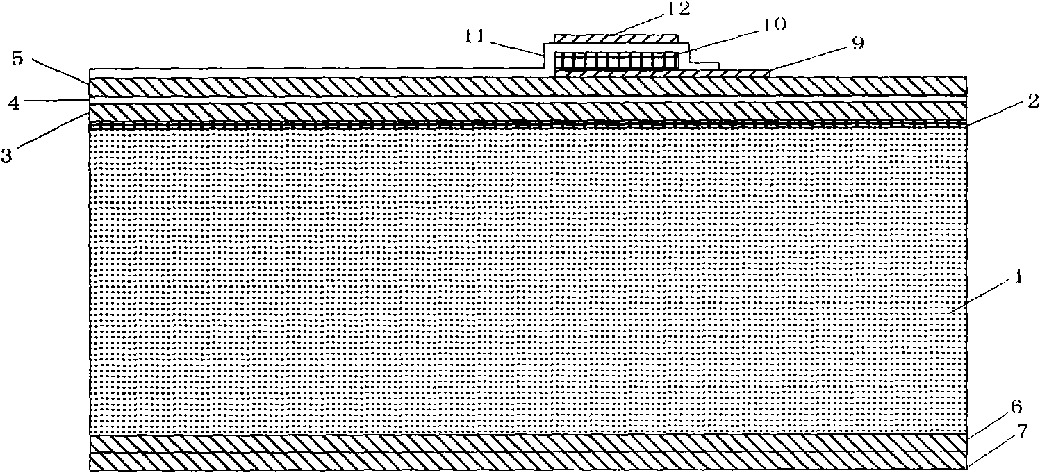
[0068] Embodiment 1, adopt preparation method of the present invention to prepare a piezoelectric microphone chip, its steps are as follows:
[0069] 1) Clean the silicon substrate 1
[0070] Cleaning the silicon substrate 1 with an acid cleaning solution and an alkaline cleaning solution respectively, and then rinsing it with deionized water;
[0071] 2) Oxide layer formation by thermal oxidation 2
[0072] On the silicon substrate 1, use a thermal oxidation furnace to oxidize the oxide layer with a thickness of 0.2 μm, and remove the oxide layer on the reverse side, so that a thermal oxide film layer 2 with a thickness of 0.2 μm is formed on the front side of the substrate 1;
[0073] 3) Low-pressure chemical vapor deposition of the first silicon nitride film layer 3
[0074] A first silicon nitride film layer 3 with a thickness of 0.5 μm on the thermal oxide film layer 2 and a third silicon nitride mask layer 6 with a thickness of 0.5 μm on the reverse side of the silicon...
Embodiment 2
[0103] Embodiment 2, using the preparation method of the present invention to prepare a novel piezoelectric microphone chip, the steps are as follows:
[0104] 1) Clean the silicon substrate 1
[0105] Cleaning the silicon substrate 1 with an acid cleaning solution and an alkaline cleaning solution respectively, and then rinsing it with deionized water;
[0106] 2) Oxide layer formation by thermal oxidation 2
[0107] On the silicon substrate 1, use a thermal oxidation furnace to oxidize the oxide layer with a thickness of 0.2 μm, and remove the oxide layer on the reverse side, so that a thermal oxide film layer 2 with a thickness of 0.2 μm is formed on the front side of the substrate 1;
[0108] 3) Low-pressure chemical vapor deposition of the first silicon nitride film layer 3
[0109] A first silicon nitride film layer 3 with a thickness of 0.5 μm on the thermal oxide film layer 2 and a third silicon nitride mask layer 6 with a thickness of 0.5 μm on the reverse side of t...
Embodiment 3
[0136] Embodiment 3, using the preparation method of the present invention to prepare a novel piezoelectric microphone chip, the steps are as follows:
[0137] 1) Clean the silicon substrate 1
[0138] Cleaning the silicon substrate 1 with an acid cleaning solution and an alkaline cleaning solution respectively, and then rinsing it with deionized water;
[0139] 2) Oxide layer formation by thermal oxidation 2
[0140] On the silicon substrate 1, use a thermal oxidation furnace to oxidize the oxide layer with a thickness of 0.2 μm, and remove the oxide layer on the reverse side, so that a thermal oxide film layer 2 with a thickness of 0.2 μm is formed on the front side of the substrate 1;
[0141] 3) Low-pressure chemical vapor deposition of the first silicon nitride film layer 3
[0142] A first silicon nitride film layer 3 with a thickness of 0.5 μm on the thermal oxide film layer 2 and a third silicon nitride mask layer 6 with a thickness of 0.5 μm on the reverse side of t...
PUM
| Property | Measurement | Unit |
|---|---|---|
| Thickness | aaaaa | aaaaa |
| Thickness | aaaaa | aaaaa |
| Thickness | aaaaa | aaaaa |
Abstract
Description
Claims
Application Information
 - R&D
- Intellectual Property
- Life Sciences
- Materials
- Tech Scout
- Unparalleled Data Quality
- Higher Quality Content
- 60% Fewer Hallucinations
Browse by: Latest US Patents, China's latest patents, Technical Efficacy Thesaurus, Application Domain, Technology Topic, Popular Technical Reports.
© 2025 PatSnap. All rights reserved.Legal|Privacy policy|Modern Slavery Act Transparency Statement|Sitemap|About US| Contact US: help@patsnap.com


