Etching method of solar battery silicon chip edges and reverse diffusion layer
A solar cell and diffusion layer technology, applied in circuits, electrical components, sustainable manufacturing/processing, etc., can solve problems such as difficulty in control, battery performance degradation, and difficulty in monitoring, to reduce peripheral defects and cracks, and reduce process debris. rate, the effect of reducing leakage
- Summary
- Abstract
- Description
- Claims
- Application Information
AI Technical Summary
Problems solved by technology
Method used
Image

Examples
Embodiment 1
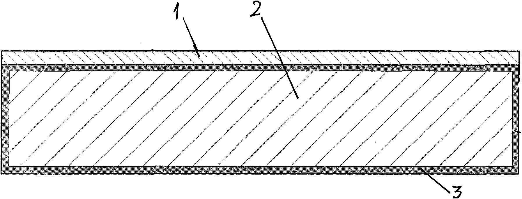
[0015] Embodiment 1, solar cell silicon wafer periphery and back diffusion layer etch, its process steps are as follows:
[0016] 1. Deposit and deposit a barrier layer mask on the front side of the solar cell silicon wafer that has been diffused to be etched using the deposition principle; the material used for the barrier layer mask is photoresist.
[0017] 2. After depositing the barrier layer mask, put the silicon wafer into the etching solution (a mixture of hydrofluoric acid and nitric acid) to allow it to react for a sufficient time (etching above 70 degrees Celsius for more than one minute) to ensure that all the diffusion parts on the back are fully reacted , take it out and clean it with deionized water; the mass ratio of hydrofluoric acid and nitric acid in the mixed solution of hydrofluoric acid and nitric acid is between 1:10 and 10:1, and the mixed solution of hydrofluoric acid and nitric acid is dissolved in an aqueous solution with a concentration of 2% by mass ...
Embodiment 2
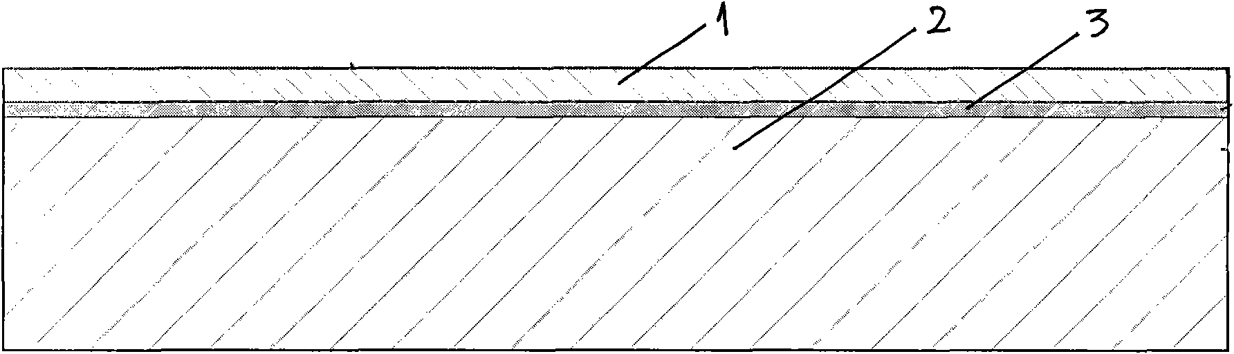
[0019] Embodiment 2, the application of the method of the present invention in the manufacture of solar cell silicon wafers with different surface topography on both sides or in different regions, the method is basically the same as in embodiment 1, except that the region of the deposition mask and the etching method are different:
[0020] 1. Take the solar cell silicon wafer that has been diffused to be etched, and use the deposition principle to select and make a barrier layer mask on the solar cell silicon wafer according to the required area; the material used for the barrier layer mask is silicon nitride, oxide silicon or titanium oxide.
[0021] 2. After depositing the barrier layer mask, put the silicon wafer into the etching solution (lye) to allow it to react for a sufficient time to ensure that the undeposited area becomes the desired shape, take it out and rinse; the OH of the lye - The ion molar concentration is between greater than 1% and the maximum solubility s...
Embodiment 3
[0023] Embodiment 3 is basically the same as Embodiment 2, except that the desired shape is first formed on the entire silicon wafer, and the desired shape is removed by etching the area, and another desired shape is etched.
[0024] 1. Take the solar cell silicon wafer that has been diffused to be etched, and use the deposition principle to select and make a barrier layer mask on the silicon wafer (the side that needs to protect the morphology) according to the required area; the barrier layer mask uses The material is silicon oxide.
[0025] 2. After depositing the barrier layer mask, put the silicon wafer into the etching solution to allow it to react for a sufficient time to ensure that the undeposited area becomes the desired shape, take it out and rinse;
[0026] 3. Put the silicon wafer in hydrofluoric acid solution to remove the barrier layer mask, take it out and wash it with deionized water.
PUM
 Abstract
Description
Claims
Application Information
 - R&D
- Intellectual Property
- Life Sciences
- Materials
- Tech Scout
- Unparalleled Data Quality
- Higher Quality Content
- 60% Fewer Hallucinations
Browse by: Latest US Patents, China's latest patents, Technical Efficacy Thesaurus, Application Domain, Technology Topic, Popular Technical Reports.
© 2025 PatSnap. All rights reserved.Legal|Privacy policy|Modern Slavery Act Transparency Statement|Sitemap|About US| Contact US: help@patsnap.com