PN type nuclear battery and preparation method thereof
A technology of nuclear batteries and batteries, applied in circuits, nuclear engineering, electrical components, etc., can solve the problems of small battery energy capacity and inability to meet long-term power supply, and achieve the effects of increasing energy density, improving energy conversion efficiency, and prolonging service life
- Summary
- Abstract
- Description
- Claims
- Application Information
AI Technical Summary
Problems solved by technology
Method used
Image
Examples
Embodiment 1
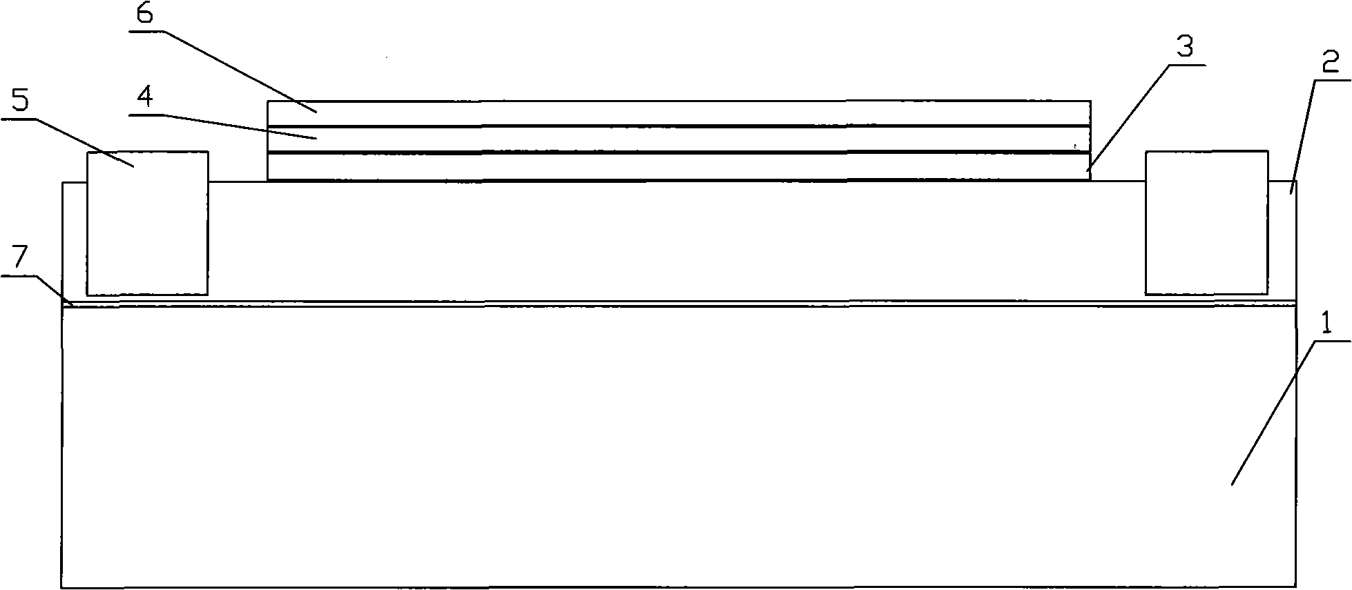
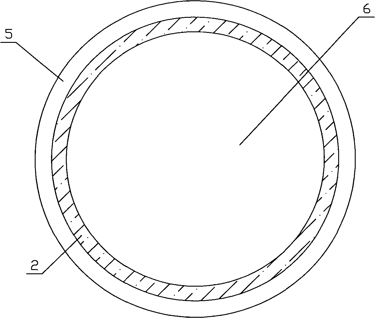
[0027] Such as figure 1 The shown schematic diagram of the structural axis section of an embodiment of the nuclear battery, first prepare the Al 2 o 3 Wafers, which can be purchased from the market to obtain single-side polished 2-inch C-side β-Al 2 o 3 The substrate 1 has a thickness of 300 μm.
[0028] Then proceed to PN wafer growth process: using MOCVD epitaxial growth equipment, Al 2 o 3 Substrate 1 is nitrided by passing through ammonia gas at 1100°C for about 2 minutes, then cooling down to 570°C, passing through trimethylgallium and ammonia gas to epitaxially form a gallium nitride (GaN) buffer layer 7 of about 20nm, and then raising the temperature to 1150°C Controlling the silicon doping concentration at 1×10 18 / cm 3 Under stable conditions, trimethylgallium, ammonia gas and silane were introduced to epitaxy an n-GaN epitaxial layer of about 2 μm, then cooled to room temperature, and the sample was taken out; the sample was put into the HVPE system, and the t...
Embodiment 2
[0031] Prepare Al first 2 o 3 Wafers, which can be purchased from the market to obtain single-side polished 2-inch C-side β-Al 2 o 3 The substrate 1 has a thickness of 400 μm.
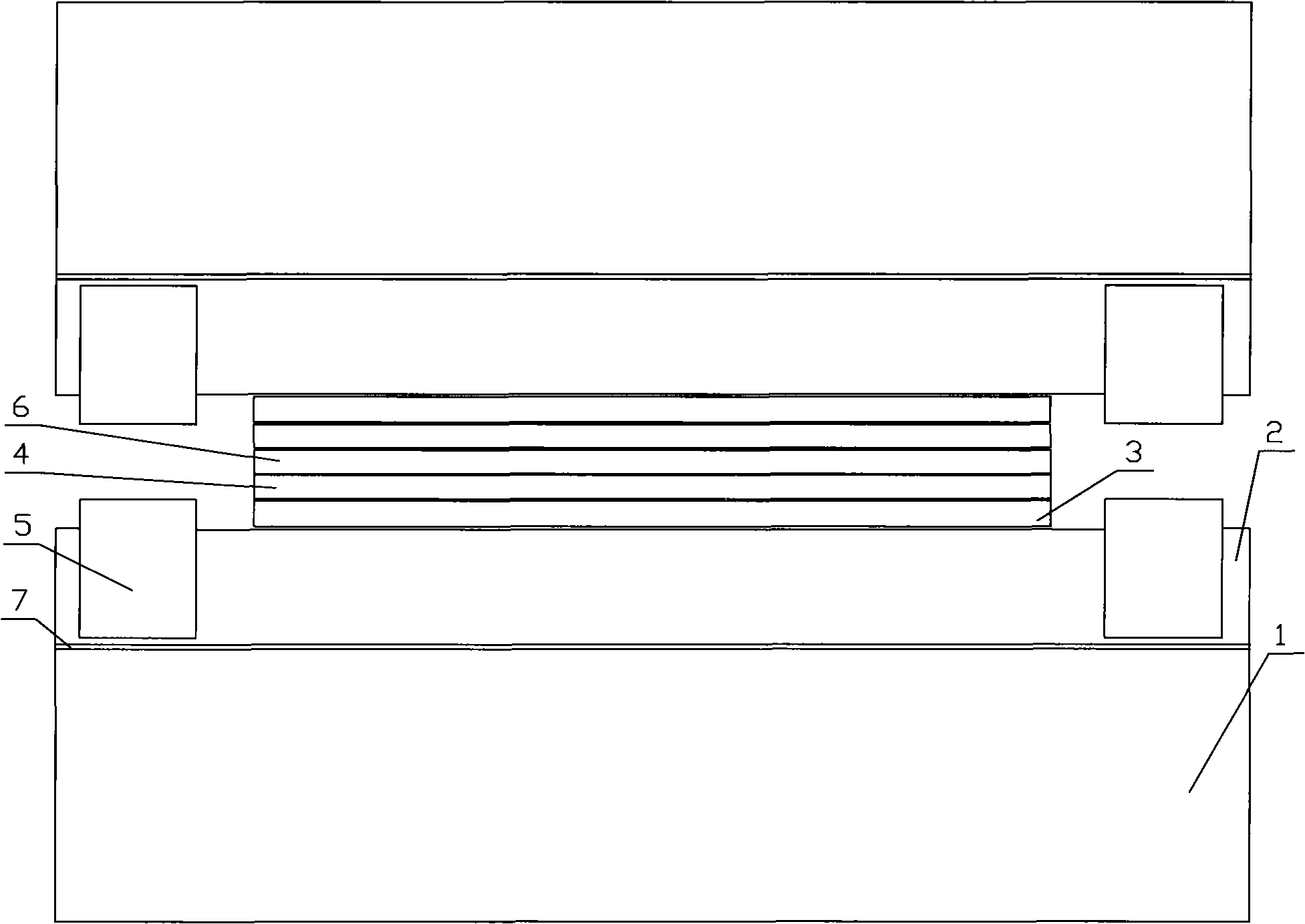
[0032] Then proceed to PN wafer growth process: using MOCVD epitaxial growth equipment, Al 2 o 3 Substrate 1 is nitrided by passing through ammonia gas at 1100°C for about 2 minutes, then cooling down to 570°C, passing through trimethylgallium and ammonia gas to epitaxially form a gallium nitride (GaN) buffer layer 7 of about 20nm, and then raising the temperature to 1150°C Controlling the silicon doping concentration at 1×10 19 / cm 3 Under stable conditions, trimethylgallium, ammonia gas and silane were introduced to epitaxy an n-GaN epitaxial layer of about 2 μm, then cooled to room temperature, and the sample was taken out; the sample was put into the HVPE system, and the temperature was raised to 1070°C to control the silicon doping concentration. in 1×10 18 / cm 3 Under stable conditions, ...
Embodiment 3
[0036] The preparation method is the same as that of the above two examples. The battery structure can be either the single structure of Example 1 or the composite structure of Example 2. The difference of this example is that the isotope layer 6 can also use nuclear waste strontium-90 , can also realize the preparation of high-efficiency radiovoltaic effect nuclear battery.
[0037] It should be noted that in all implementations including the above three examples, the total thickness of the p-type GaN doped layer and the p-type contact electrode cannot exceed 40nm (for the case described in Example 2, one side is used for calculation) , otherwise it will affect the conversion efficiency of the nuclear battery. Moreover, different nuclear batteries can be integrated in a certain way to obtain higher voltage or current nuclear batteries to meet the needs of different situations.
[0038] From the point of view of expanded application, the micro-energy layout (each nuclear cell...
PUM
 Abstract
Description
Claims
Application Information
 - R&D Engineer
- R&D Manager
- IP Professional
- Industry Leading Data Capabilities
- Powerful AI technology
- Patent DNA Extraction
Browse by: Latest US Patents, China's latest patents, Technical Efficacy Thesaurus, Application Domain, Technology Topic, Popular Technical Reports.
© 2024 PatSnap. All rights reserved.Legal|Privacy policy|Modern Slavery Act Transparency Statement|Sitemap|About US| Contact US: help@patsnap.com


