
Molding circuit component and process for producing the same

A technology for forming circuits and manufacturing methods, which is applied in the fields of printed circuit manufacturing, printed circuit components, printed circuits, etc., can solve the problems of reduced yield rate, limited application field, and difficulty in widening the width of the non-forming surface 10c of the circuit, and achieves Effects of preventing short circuits and widening the utilization area

Inactive Publication Date: 2008-09-10
SANKYO KASEI CO LTD
View PDF0 Cites 2 Cited by
  • Summary
  • Abstract
  • Description
  • Claims
  • Application Information

AI Technical Summary

Problems solved by technology

In addition, there is a problem that it is limited to the case of a large non-circuit width, and there is also a difference in the material characteristics of the primary substrate 10, that is, the high-frequency characteristics and the material of the resin mask 30, which are required in the field of use of the molded circuit components of the finished product. Exploit domain-limited issues
[0010] For example, for the compatibility of the material of the primary substrate 10 and the material of the resin mask 30 of the secondary substrate 20, the high-frequency characteristics and dielectric properties of the primary substrate 10 On the premise of a constant value, it is often difficult to select a resin mask 30 with good compatibility with the material of the primary substrate 10. In reality, it is often impossible to select a primary substrate 10 with good compatibility.
Moreover, if the compatibility is poor, even if the circuit-forming surface 10b of the roughened primary substrate 10 is exposed, other circuit-non-forming surfaces 10c such as Figure 8 as well as Figure 7 Covered by a resin mask 30 as shown in (C), as Figure 9 as well as Figure 7 As shown in (D), when immersed in the catalyst solution for electroless plating, the catalyst solution penetrates into the circuit non-formation surface 10c covered by the resin mask 30, so the metal plating is deposited to cause a short circuit between the circuits, and the yield decline
[0011] In order to prevent such a short circuit between circuits, it is currently solved by widening the width of the circuit non-formation surface 10c. However, as will be described later, there has been a strong demand for It is extremely difficult to widen the width of the non-circuit formation surface 10c in the current situation of narrowing the wiring interval, for example, forming a 200μm interval

Method used


Image

  • Molding circuit component and process for producing the same
  • Molding circuit component and process for producing the same
  • Molding circuit component and process for producing the same

Examples


Embodiment 1

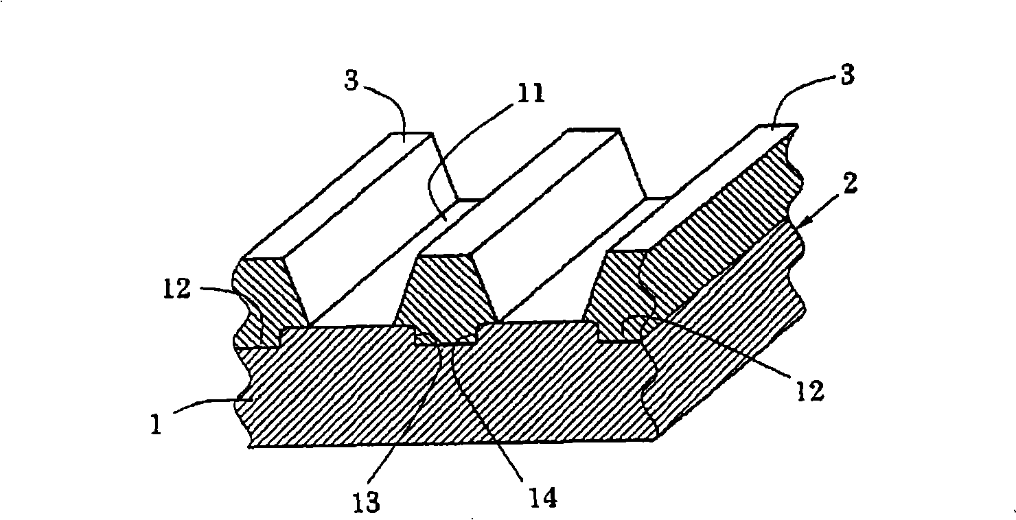
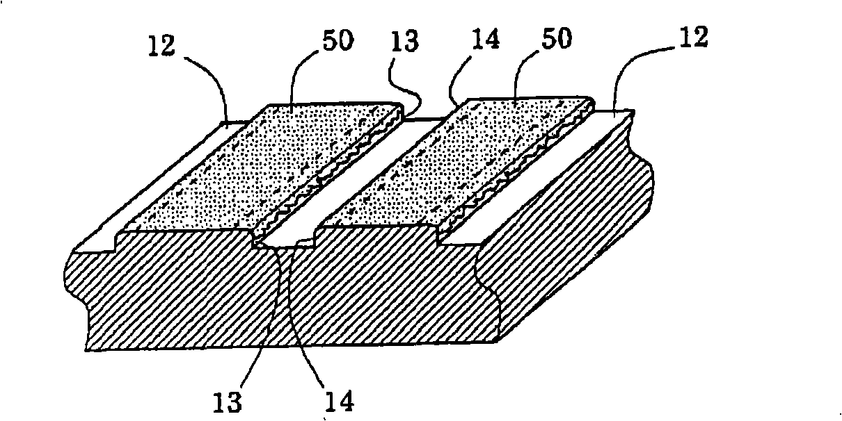
[0046] refer to Figure 1 ~ Figure 3 Illustrate the embodiment of the present invention, in figure 1 Among them, the primary substrate 1 is formed by injection molding the "VECTRA C820" of liquid crystal polymer. Its shape is that the circuit forming surface 11 is convex, and the circuit non-forming surface 12 is concave, and the height difference is formed as 0.05mm. The angle of the side walls 13 and 14 connecting the circuit-forming surface and the circuit-non-forming surface is formed at 90°. Furthermore, the surface of the primary substrate 1 is roughened with a caustic soda solution.

[0047] The circuit forming surface 11 on which the conductive layer 50 is formed is exposed, and the resin mask 3 covering the concave circuit non-forming surface 12 is injection-molded. The state of about mm. As the material of the resin mask 3, "ECOMATY AX-2000" of the said Nippon Gosei Kagaku Kogyo of polyvinyl alcohol system was used.

[0048] In order to apply the catalyst, the s...

Embodiment 2

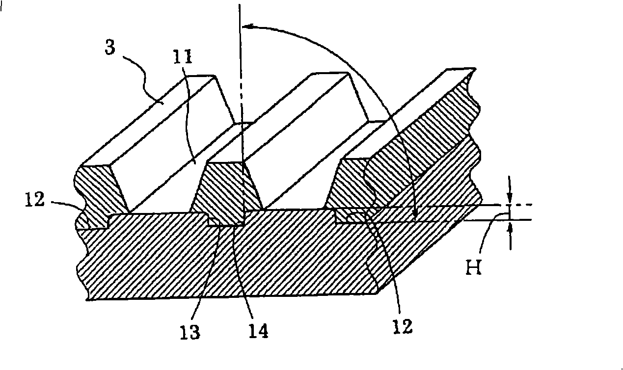
[0060] refer to Figure 4 ~ Figure 6 Illustrate embodiment 2 of the present invention, in image 3 The primary substrate 6 is formed by injection molding the "VECTRA C820" of liquid crystal polymer. Its shape is that the circuit forming surface 61 is concave, and the circuit non-forming surface 62 is convex, and its height difference H is as follows: Image 6 It is shown that the formation is 0.2 mm, and the inclination angle of the non-circuit formation portion is formed at 80°. Furthermore, the surface of the primary substrate 6 is roughened with a caustic soda solution.

[0061] The circuit-forming surface 61 on which the conductive layer 50 is formed is exposed, and the resin mask 31 covering the convex non-circuit-forming surface 62 is injection-molded. , forming the secondary matrix 2 in the coated state. As the material of the resin mask 31, "ECOMATY AX-2000" of the said Nippon Gosei Kagaku Kogyo of polyvinyl alcohol system was used.

[0062] In order to apply the c...


PUM

PropertyMeasurementUnit
Circuit widthaaaaaaaaaa

Abstract

The range of selection of the material for a primary substrate and the material for a resin mask in a secondary substrate can be broadened, and short circuiting of a circuit can be reliably prevented. The shape of a primary substrate (1) is such that a circuit forming face (11) is in a convex form and a circuit non-forming face (12) is in a concave form, the difference in level between the circuit forming face (11) and the circuit non-forming face (12) is 0.05 mm, and the angle of side walls (13, 14) connecting the circuit forming face to the circuit non-forming face is 90 . In order to apply a catalyst, a palladium catalyst solution was immersed in a bath having a water depth of 500 mm at a liquid temperature of 40 C for 5 min. Thereafter, a resin mask (3) is dissolved and removed, followed by electroless plating. As a result, the catalyst solution penetrates up to a part in which the creeping distance could have been increased, that is, up to both side walls (13, 14). That is, the catalyst penetration can be prevented, and short circuiting between conductive layers (50), that is, between circuits, can be prevented.

Description

technical field [0001] The present invention relates to a molded circuit component in which a circuit is formed by plating a part of the surface or the inner peripheral surface of a through hole in, for example, a connector for a mobile phone, and a method for manufacturing the same. Background technique [0002] The inventors of this application have previously proposed Figure 7 ~ Figure 9 The manufacturing method of the shaped circuit part is shown. Here, for the description of the manufacturing method, first, as Figure 7 As shown in (A), the primary base 10 , which is a circuit-formed body of a predetermined shape, is electrically insulatingly molded by injection molding a thermoplastic material. The conductive layer 50 formed on the upper surface of the primary substrate 10 (refer to Figure 7 , F), that is, a flat surface on which the circuit formation surface and other circuit non-formation surfaces (non-circuit surfaces) are at the same level. As the thermoplasti...

Claims


Application Information

Patent Timeline
IPC IPC(8): H05K3/18H05K3/00B29C69/00
CPCH05K1/0256H05K3/184H05K2201/0761H05K2201/09036H05K2201/09045H05K2201/09118H05K2203/0565Y10T428/24479
Inventor 吉泽德夫渡边浩聪
Owner SANKYO KASEI CO LTD
Learn More