Method for etching tungsten-silicide silicon-die

A technology of tungsten silicide silicon wafers and tungsten silicide, which is applied in the fields of electrical components, semiconductor/solid-state device manufacturing, circuits, etc., can solve the problems of many steps, too many particles and defects, etc., so as to improve yield rate, reduce etching steps, The effect of improving productivity

Active Publication Date: 2008-06-25
BEIJING NAURA MICROELECTRONICS EQUIP CO LTD
View PDF0 Cites 0 Cited by
  • Summary
  • Abstract
  • Description
  • Claims
  • Application Information

AI Technical Summary

Problems solved by technology

[0009] In this etching method, there are many steps in the etching process, and it is easy to produce too many particles and defects during the etching process.

Method used


Image

  • Method for etching tungsten-silicide silicon-die
  • Method for etching tungsten-silicide silicon-die
  • Method for etching tungsten-silicide silicon-die

Examples


Embodiment Construction

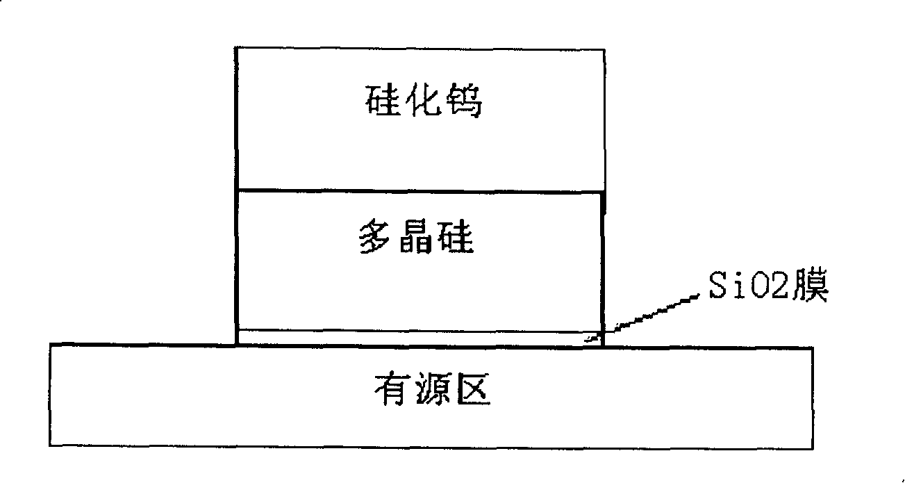
[0029] The method for etching a tungsten silicide silicon chip of the present invention is used for etching process lines on a tungsten silicide silicon chip, and the tungsten silicide silicon chip mainly includes a tungsten silicide layer and a polysilicon layer.

[0030] The etching process of the tungsten silicide silicon chip is completed in the reaction chamber. The upper radio frequency power supply and the lower radio frequency power supply are arranged on the reaction chamber, and the tungsten silicide silicon chip is installed in the reaction chamber. The process gas is filled into the reaction chamber according to the flow rate and pressure required by the etching process. At the same time, the upper RF source ionizes the process gas filled into the reaction chamber into plasma, and the lower RF source accelerates the plasma to bombard the surface of the silicon wafer to achieve Etching of silicon wafers.

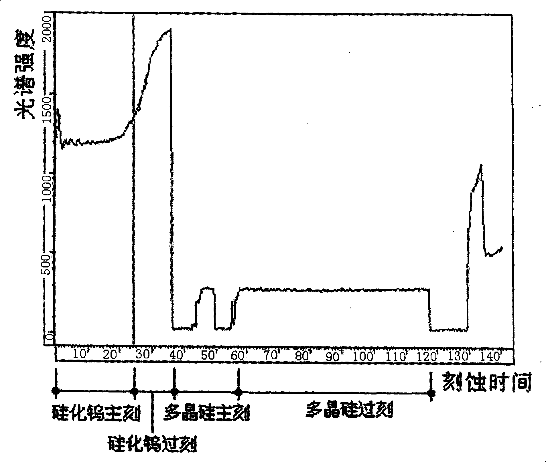
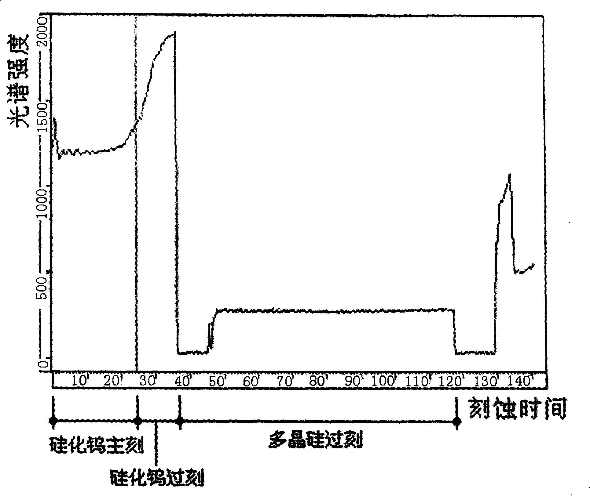
[0031] Its preferred specific implementation is as image 3...


PUM


Abstract

The invention discloses a method of etching the tungsten silicide silicon chips, which is used for etching process lines on a tungsten silicide silicon chip. The method comprises the following steps: tungsten silicide main etching, tungsten silicide excessive etching and polysilicon excessive etching, the tungsten silicide excessive etching and the polysilicon main etching in the prior art are combined into one step, thus reducing the etching steps, further reducing the particulate pollution and defects generated during the technological process, improving the defect-free rate of the silicon chip, and improving the production efficiency. The invention is mainly suitable for etching the tungsten silicide silicon chips, and is also suitable for etching other metal silicide silicon chips.

Description

technical field [0001] The invention relates to a semiconductor processing technology, in particular to a method for etching tungsten silicide silicon wafers. Background technique [0002] Advanced integrated circuit technology requires high integration, fast execution speed and stable performance of semiconductor components. At present, the delay time to the element has been reduced by changing the semiconductor structure of the element, thereby increasing the execution speed of the element. For elements with a metal oxide semiconductor structure, a conductive layer with a lower resistivity is usually added to the general gate structure. This conductive layer uses metal silicide, which has the characteristics of low resistance, anti-electron migration, and high melting point. The elements commonly used to form metal silicides are: titanium, molybdenum, tantalum, tungsten, etc. Since tungsten silicide has strong covalent bonding, better resistance to electron migration, t...

Claims


Application Information

Patent Timeline
Patent Type & Authority Applications(China)
IPC IPC(8): H01L21/3213
Inventor 王铮
Owner BEIJING NAURA MICROELECTRONICS EQUIP CO LTD
Why Eureka
Try Eureka