Core-skin structure micropore silicon carbide fiber and method for producing the same
A technology of silicon carbide fiber and microporous silicon carbide, which is applied in the fields of fiber chemical characteristics, melt spinning, textiles and papermaking, and can solve the problems of low fiber specific surface area, low efficiency, and no skin-core structure.
- Summary
- Abstract
- Description
- Claims
- Application Information
AI Technical Summary
Problems solved by technology
Method used
Image
Examples
Embodiment 1
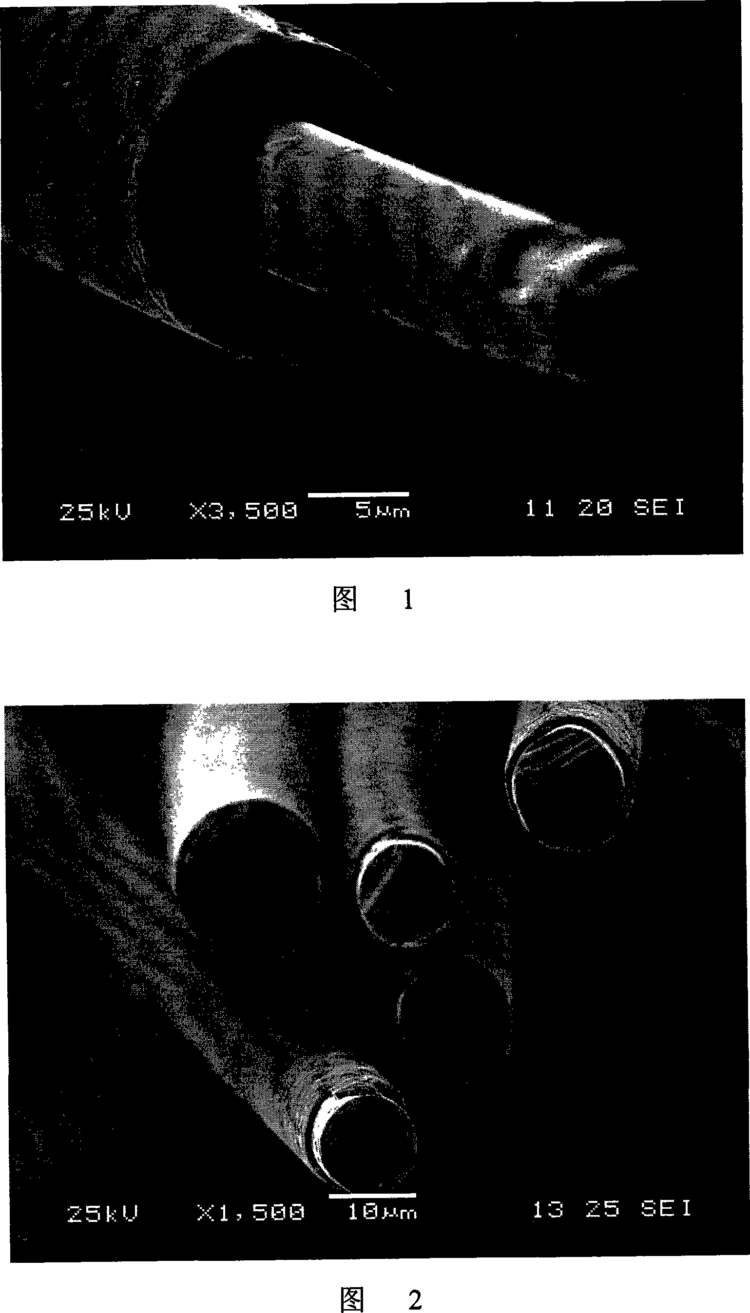
[0022] The microscopic morphology of the silicon carbide fiber in this example is shown in Figure 1, and the specific surface area is 1100 m 2 / g, the average pore size is 1.42 nm, the thickness of the skin layer is 4.8 μm, and the ratio to the radius is 0.80. The energy spectrum analysis shows that the contents of C, Si, and O in the skin layer are 94wt%, 1wt%, and 5wt%, respectively. The content of , O is 30wt%, 55wt%, 15wt%, respectively. The resistivity of the fiber is 3×10 -2 Ω·cm.
[0023] Preparation: (1) Take 10g of PCS and put it in a melt spinning device, heat it to 290°C under the protection of high-purity nitrogen with a purity of ≥99%, and carry out defoaming treatment, then at 260°C, under a pressure of 0.5MPa, at a pressure of 120 m / m Melt spinning at a speed of min to obtain a 15μm diameter precursor; (2) place the precursor in an oxidation furnace, heat it to 200°C at a heating rate of 15°C / h in an air atmosphere, and keep it for 2 hours to obtain oxygen In...
Embodiment 2
[0025] The microscopic morphology of the silicon carbide fiber in this example is shown in Figure 2, and the specific surface area is 510 m 2 / g, the average pore size is 1.35 nm, the thickness of the skin layer is 0.6 μm, and the ratio to the radius is 0.10. The energy spectrum analysis shows that the contents of C, Si, and O in the skin layer are 92wt%, 3wt%, and 5wt%, respectively. The content of , O is 30wt%, 55wt%, 15wt%, respectively. The resistivity of the fibers was 10 Ω·cm.
[0026] Preparation: The activation treatment time of step (4) in this example is 0.5h, and the rest are the same as those in Example 1.
Embodiment 3
[0028] The specific surface area of the silicon carbide fiber in this embodiment is 1400m 2 / g, the average pore size is 1.55nm, the thickness of the skin layer is about 5.4μm, and the ratio to the radius is 0.90. The energy spectrum analysis shows that the content of C, Si, and O in the skin layer are 96wt%, 0wt%, and 4wt%, respectively. The contents of Si and O were 31 wt %, 54 wt %, and 15 wt %, respectively. The resistivity of the fiber is 5×10 -3 Ω·cm.
[0029] Preparation: step (4) in this example, the activation treatment time is 15h, and the rest are the same as in Example 1.
PUM
| Property | Measurement | Unit |
|---|---|---|
| pore size | aaaaa | aaaaa |
| pore size | aaaaa | aaaaa |
| thickness | aaaaa | aaaaa |
Abstract
Description
Claims
Application Information
 - Generate Ideas
- Intellectual Property
- Life Sciences
- Materials
- Tech Scout
- Unparalleled Data Quality
- Higher Quality Content
- 60% Fewer Hallucinations
Browse by: Latest US Patents, China's latest patents, Technical Efficacy Thesaurus, Application Domain, Technology Topic, Popular Technical Reports.
© 2025 PatSnap. All rights reserved.Legal|Privacy policy|Modern Slavery Act Transparency Statement|Sitemap|About US| Contact US: help@patsnap.com

