Method for manufacturing machine-direction double-grid metal-oxide-semiconductor element

An oxide and gate metal technology is applied in the field of manufacturing vertical double-gate MOS devices based on silicon-on-insulator materials, which can solve the problems of small overlapping area of ​​modulation area and light field, and the modulation efficiency needs to be improved, and achieves the effect of reducing the complexity of process fabrication

Inactive Publication Date: 2008-05-07
INST OF SEMICONDUCTORS - CHINESE ACAD OF SCI
View PDF0 Cites 3 Cited by
  • Summary
  • Abstract
  • Description
  • Claims
  • Application Information

AI Technical Summary

Problems solved by technology

The MOS structure avoids the influence of the carrier recombination process on the modulation rate of the device, but the overlapping area of ​​the modulation area and the light field is small, and the modulation efficiency needs to be improved.

Method used


Image

  • Method for manufacturing machine-direction double-grid metal-oxide-semiconductor element
  • Method for manufacturing machine-direction double-grid metal-oxide-semiconductor element
  • Method for manufacturing machine-direction double-grid metal-oxide-semiconductor element

Examples


Embodiment

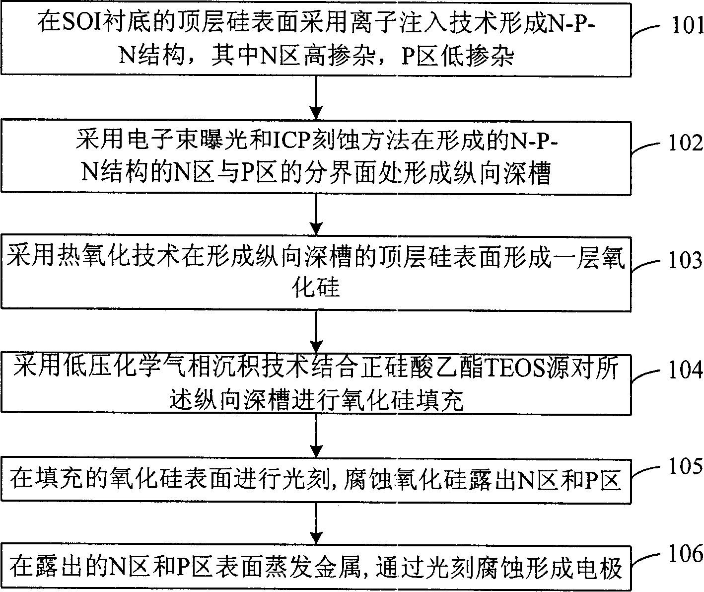
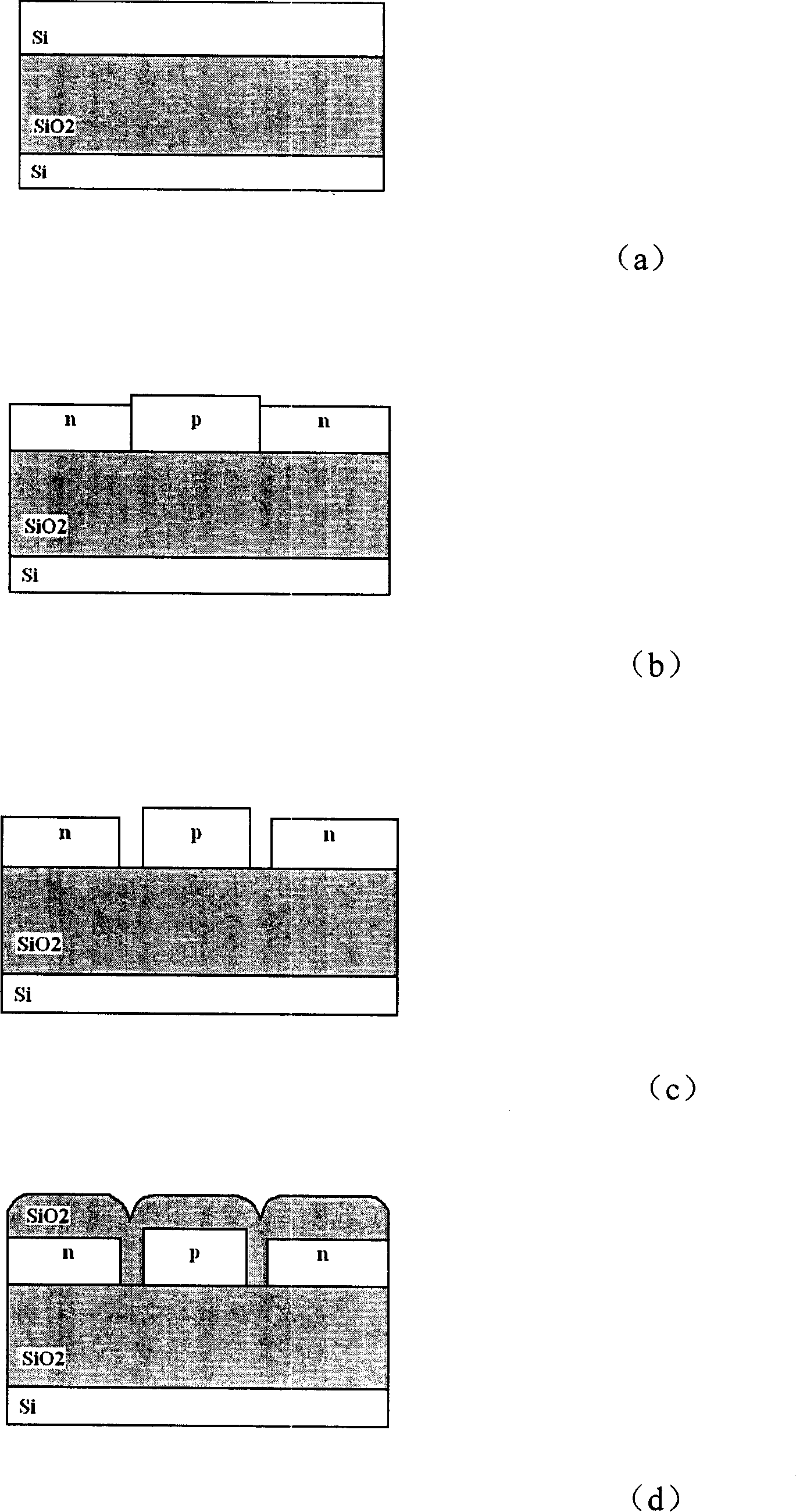
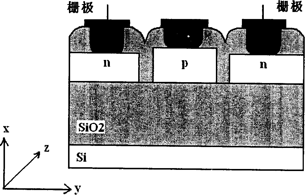
[0056] Such as figure 2 as shown, figure 2 In order to produce a process flow diagram of a vertical double-gate MOS device according to an embodiment of the present invention, the method specifically includes the following steps:

[0057] First, the SOI substrate is cleaned. Such as figure 2 As shown in Figure a, Figure a is a schematic structural view of the SOI substrate used in the present invention.

[0058] Second, perform ordinary photolithography on the cleaned SOI substrate. It is assumed that the top silicon of the SOI substrate itself is P-type low-doped (if the concentration and type of the top silicon do not meet the requirements, large-area ion implantation can be used to obtain a rational concentration). Use photoresist as a mask to perform shallow etching of silicon and ion implantation to form a highly doped N region, which is used as an ohmic contact electrode at the end. The purpose of shallow etching silicon is to leave marks for the next step of ele...


PUM


Abstract

The invention discloses a method for manufacturing a longitudinal dual-grid MOS component, which comprises the following steps: firstly, an ion implantation technology is adopted on a silicon face at the top layer of a SOI substrate to form an N-P-N structure, wherein an N area is highly doped, and a P area is lowly doped; secondly, an electron beam exposure method and an ICP etching method are adopted to form a longitudinal trench at the position of the interface of the N area and the P area where the N-P-N structure is formed; thirdly, a thermal oxidation technology is adopted to form a layer of silicon oxide on the silicon face at the top layer of the longitudinal trench; fourthly, a low pressure chemical vapor deposition technology is adopted to combine a tetra ethyl ortho silicate TEOS source to be filled with the silicon oxide to the longitudinal trench; fifthly, the photoetching is operated on the surface of the filled silicon oxide, the silicon oxide is corroded and the N area and the P area are exposed; sixthly, metal is evaporated on the surface of the exposed N area and P area, and an electrode is formed through the photoetching corrosion. Through adopting the invention, the high speed information transmission in the optical communication and inside a chip system is realized.

Description

technical field [0001] The invention relates to the technical field of vertical double-gate metal-oxide-semiconductor (MOS) devices in semiconductor devices, in particular to a method for manufacturing a vertical double-gate MOS device based on silicon-on-insulator (SOI) material. Background technique [0002] In recent years, with the rapid development of silicon-on-insulator-compensated metal-oxide-semiconductor (SOI CMOS) technology and SOI optical waveguide devices, people have continuously turned their attention to the multifunctional integration of SOI-based on-chip optoelectronic devices. [0003] SOI technology has incomparable advantages over bulk silicon technology. CMOS devices made on SOI materials have the advantages of low power consumption, strong anti-interference ability, high integration, high speed, simple process, and strong anti-radiation ability. As the thickness of the top silicon film of SOI is reduced to less than the width of the depletion region o...

Claims


Application Information

Patent Timeline
Patent Type & Authority Applications(China)
IPC IPC(8): H01L21/336H01L21/28
Inventor 屠晓光陈少武
Owner INST OF SEMICONDUCTORS - CHINESE ACAD OF SCI
Why Eureka
Try Eureka