Semiconductor device and manufacturing method thereof
A technology of semiconductors and devices, applied in the field of manufacturing semiconductor devices with field effect transistors
- Summary
- Abstract
- Description
- Claims
- Application Information
AI Technical Summary
Problems solved by technology
Method used
Image
Examples
Embodiment approach 1
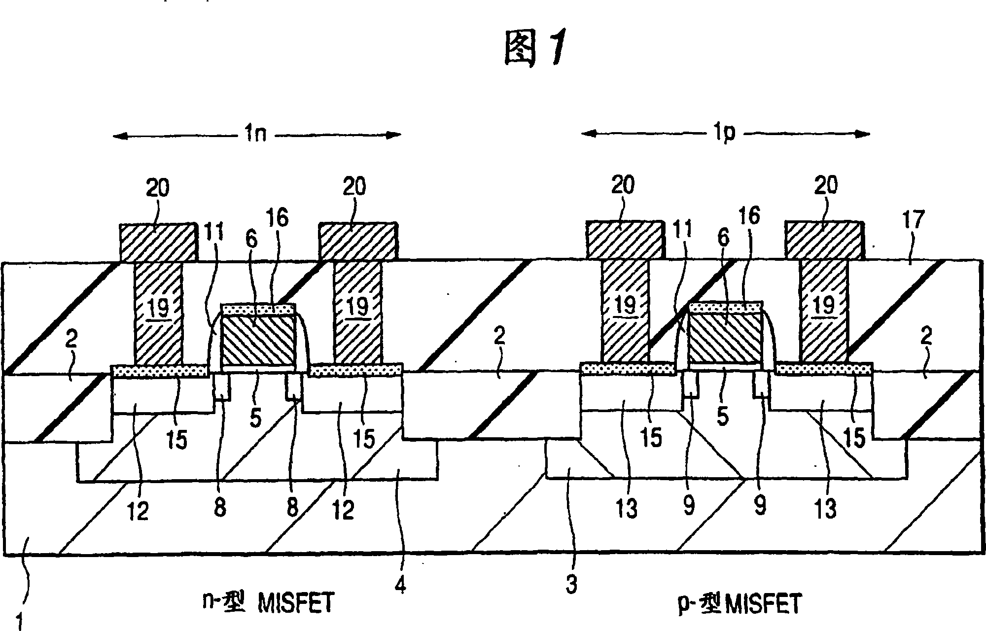
[0161] Embodiment Mode 1 describes an example in which the present invention is applied to a semiconductor device having complementary MISFETs.
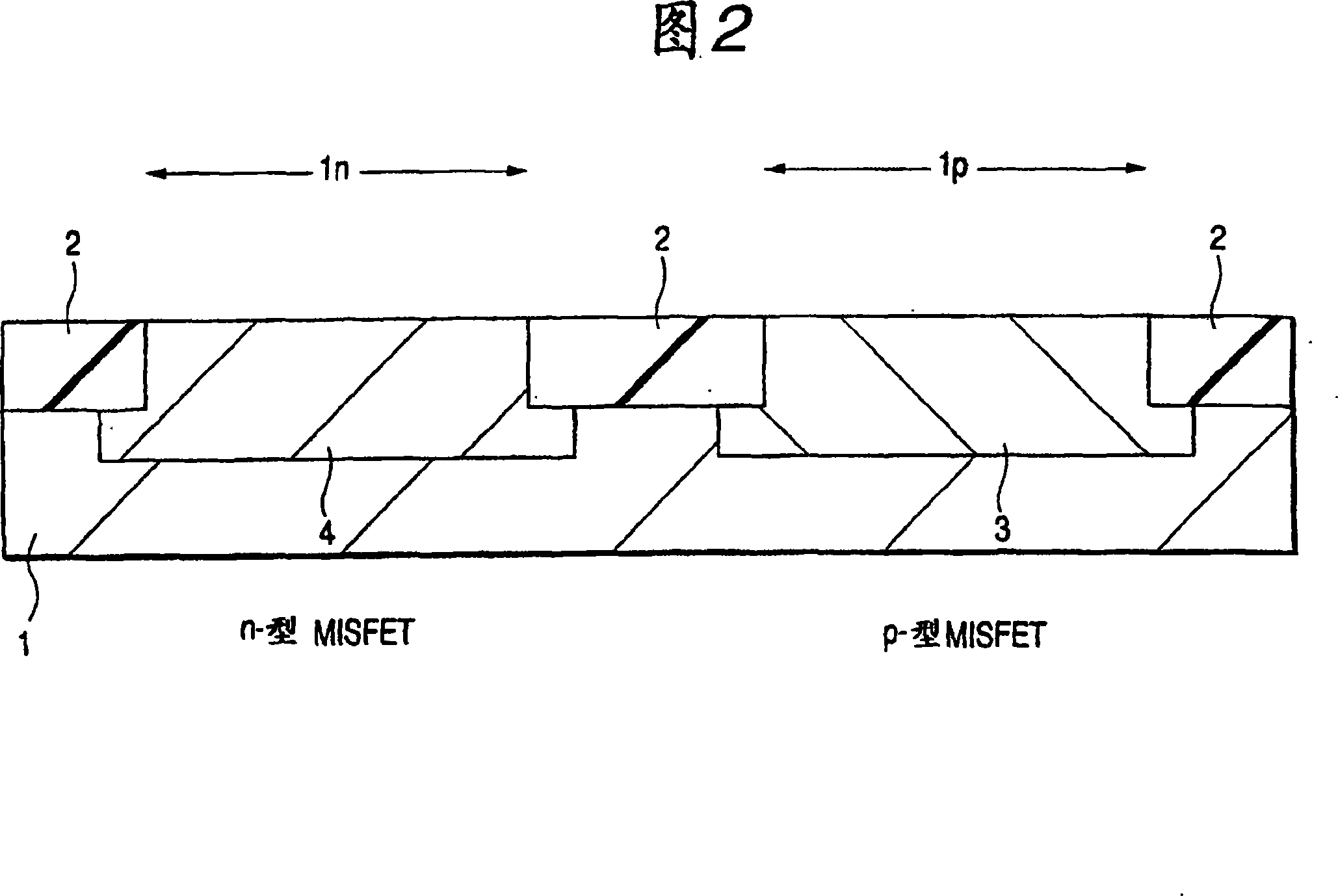
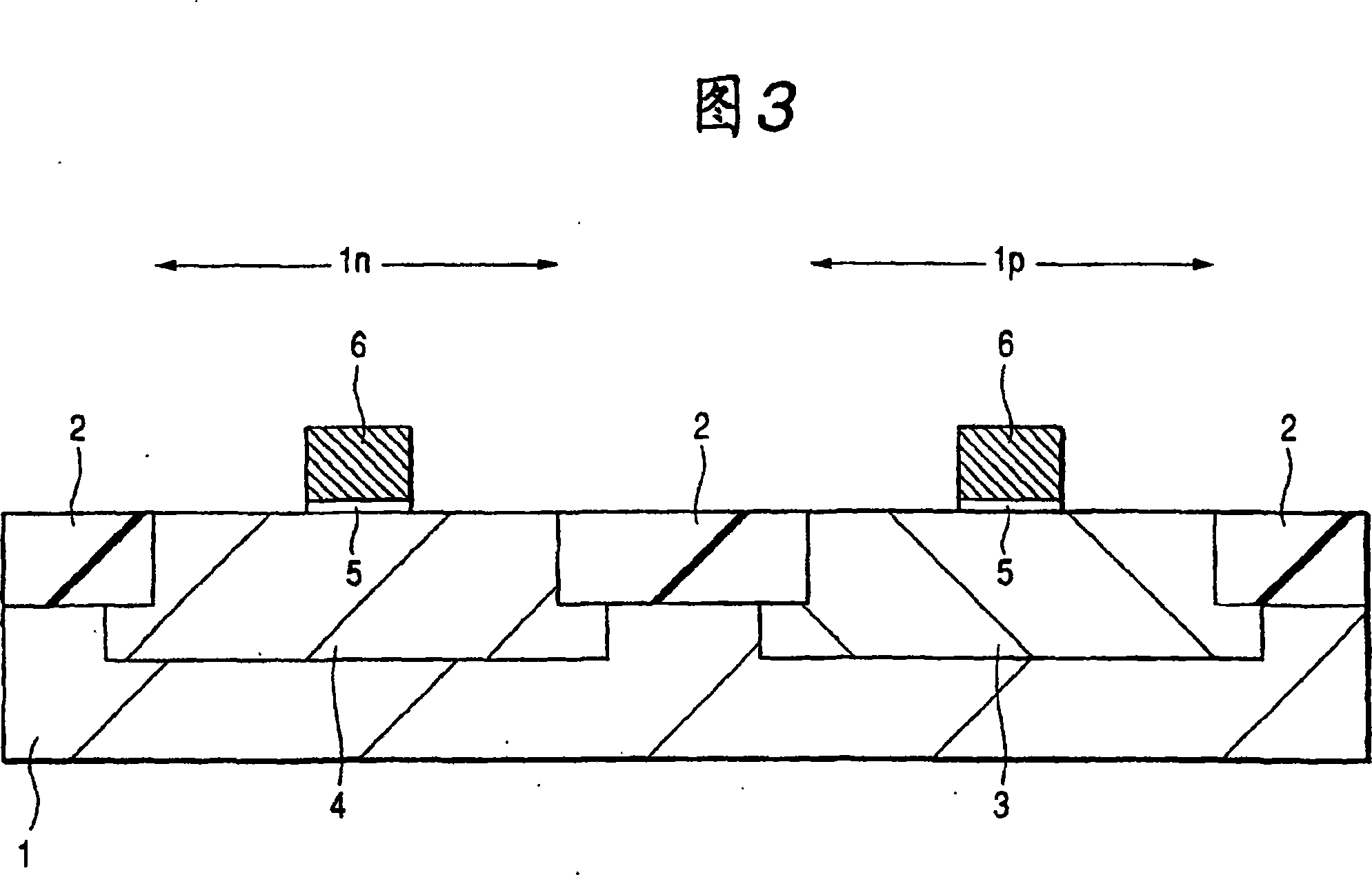
[0162] FIG. 1 is a cross-sectional view showing a schematic structure of a complementary MISFET incorporated in a semiconductor device of Embodiment 1. Referring to FIG. In FIG. 1, an n-type MISFET is shown on the left, and a p-type MISFET is shown on the right.
[0163] As shown in FIG. 1 , the semiconductor device of Embodiment Mode 1 mainly includes, as a semiconductor substrate (silicon layer as a semiconductor substrate) 1 , for example, a p-type single crystal silicon substrate.
[0164] Device fabrication regions 1n and 1p are arranged on the main surface (device fabrication surface or circuit fabrication surface) of the silicon substrate 1, which are isolated from each other by the device isolation region 2, and a p-type well region 4 and an n-type well region 4 are formed in the device fabrication region 1n. MISFET, and an ...
Embodiment approach 2
[0227] 22 to 24 are schematic cross-sectional views illustrating the manufacturing steps of the semiconductor device according to Embodiment 2 of the present invention.
[0228] In Embodiment Mode 2, it is described that the condensation of the refractory metal is suppressed during silicidation.
[0229] After the contact regions (semiconductor regions 12, 13) of the n-type and p-type MISFETs are fabricated using the same process as that of the first embodiment, as shown in FIG. and 1p internal ion implantation of group IV elements, eg, Ge, as shown in Figure 23. By the ion implantation of Ge, Ge is introduced into the contact region in addition to the Ge ions implanted before the step of forming the extension region.
[0230] Then, heat treatment is used to activate the impurity (As, BF 2 ). The heat treatment was performed under the same conditions as in Embodiment 1 above.
[0231] In this step, since the Ge ions implanted in the step of making the extension region and ...
Embodiment approach 3
[0238] In this embodiment mode, an example of applying the present invention to a semiconductor device having complementary MISFETs and DRAM (Dynamic Random Access Memory) type memory cells on the same substrate is described.
[0239] Fig. 25 shows the schematic structure of the semiconductor device of Embodiment 3 (Fig. 25(a) is a schematic cross-sectional view of a complementary MISFET, and Fig. 25(b) is a schematic cross-sectional view of a memory cell selecting a MISFET), and Fig. 26 is a schematic cross-sectional view of a memory cell installed in the implementation mode. An equivalent circuit diagram of a memory cell in the semiconductor device of Embodiment 3. FIG. 27 is a schematic cross-sectional view showing the manufacturing steps of the semiconductor device of Embodiment 3. FIG. In 25(a), the device fabrication region 1n on the left is an n-type MISFET, and the device fabrication region 1p on the right is a p-type MISFET.
[0240] As shown in FIG. 26, memory cells ...
PUM
| Property | Measurement | Unit |
|---|---|---|
| Resistivity | aaaaa | aaaaa |
Abstract
Description
Claims
Application Information
 - R&D Engineer
- R&D Manager
- IP Professional
- Industry Leading Data Capabilities
- Powerful AI technology
- Patent DNA Extraction
Browse by: Latest US Patents, China's latest patents, Technical Efficacy Thesaurus, Application Domain, Technology Topic, Popular Technical Reports.
© 2024 PatSnap. All rights reserved.Legal|Privacy policy|Modern Slavery Act Transparency Statement|Sitemap|About US| Contact US: help@patsnap.com


