
Plasma display panel and method for manufacturing same

A plasma and display panel technology, applied in the direction of AC plasma display panels, cold cathode manufacturing, electrode system manufacturing, etc., can solve the problems of insufficient power consumption, difficulty in improving luminous efficiency, high discharge start voltage, etc., and achieve the purpose of suppressing electrostatic capacitance Effects of increasing and reliably starting sustaining discharge and lowering discharge start voltage

Inactive Publication Date: 2007-09-19
PANASONIC CORP
View PDF4 Cites 0 Cited by
  • Summary
  • Abstract
  • Description
  • Claims
  • Application Information

AI Technical Summary

Problems solved by technology

[0032] However, the invention described in Patent Document 1 does not show the contribution of the invention to the withstand voltage, the discharge start voltage, and the luminous efficiency. Dielectric layers are formed by stacking materials. Therefore, different target materials or different film formation conditions are required when forming each layer, resulting in a complicated thin film process, and it is difficult to achieve reliable and stable manufacturing.
Further, using 80% SiO 2 glass and Al 2 o 3 The dielectric layer formed by vacuum evaporation or sputtering still has low density and low insulation withstand voltage. Therefore, in order to increase the withstand voltage, the film thickness of the dielectric layer must be increased. As a discharge unit, a high discharge start voltage and a high discharge maintenance voltage are required. , the problem is that it is difficult to improve the luminous efficiency
[0033] In addition, in the invention described in Patent Document 2, a metal oxide is formed on the Ag electrode after coating and firing by CVD or the like, and a dielectric layer made of dielectric glass is formed thereon. The electrodes are formed of metal oxides by CVD, and furthermore, since the dielectric layer is laminated and fired, it is difficult to prevent the generation of bubbles, etc., and the thin film process and printing process are used as the process of forming the dielectric layer, but these processes include exposure to The process in the air, so the dielectric layer will adsorb impurity gas, the problem is that it is difficult to stably manufacture a reliable PDP
[0034] In addition, in any of the inventions described in the above-mentioned Patent Documents 1 and 2, since the protective film is exposed to the air after forming the protective film by a thin film process, there is a problem of adsorption of impurity gases in the air.
[0035] That is, metal oxides such as MgO constituting the protective film have adsorbed water (H 2 O) or carbon dioxide (CO 2 ) and other impurity gases are easily degenerated into hydroxide compounds or carbonate compounds. Therefore, a PDP with a protective film mainly composed of MgO degraded into hydroxide compounds or carbonate compounds is not the same as a PDP with a protective film mainly composed of MgO. Compared with the PDP of the film, its secondary electron emission efficiency is low, so there is a problem that the discharge start voltage increases and the sputtering resistance characteristic decreases
[0036] In addition, in the invention described in the above-mentioned Patent Document 3, the discharge start voltage required to reliably start the sustain discharge is about 180 V, which is still high, and it is not enough for the requirement of reducing the power consumption of the PDP.
[0037] In addition, if the discharge delay can be reduced, the sustain discharge can be reliably started even if the discharge start voltage is lowered; however, in the invention described in the above-mentioned Patent Document 4, although the discharge delay can be reduced, on the other hand, it is necessary to set the voltage When the secondary display electrode pair 801 discharges, the main display electrode pair 802 also discharges at the same time. Therefore, as a result, it is necessary to set a higher voltage value for sustain discharge, and the discharge start voltage is as high as about 180V, which is for Insufficient for the reduction of power consumption required by PDP

Method used

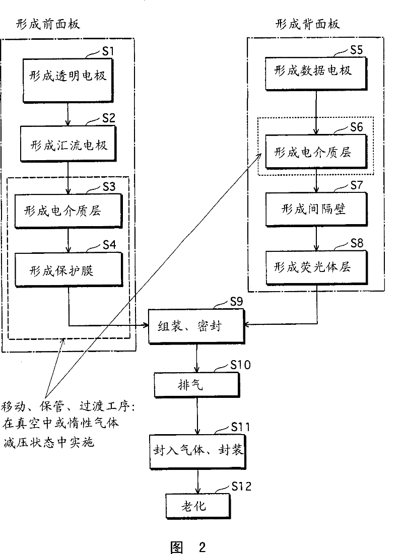
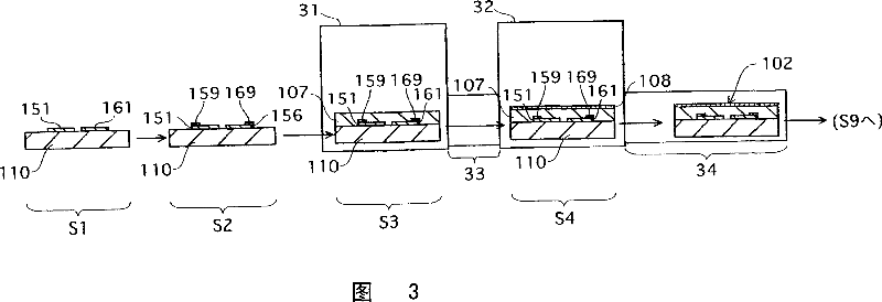

Image

  • Plasma display panel and method for manufacturing same
  • Plasma display panel and method for manufacturing same
  • Plasma display panel and method for manufacturing same

Examples


no. 1 Embodiment approach

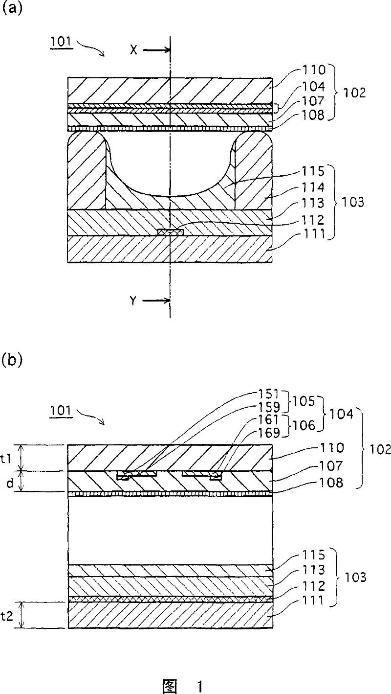
[0118] FIG. 1(a) is a cross-sectional view of the unit discharge cell of the PDP 101 in the first embodiment of the present invention, which is cut along a plane perpendicular to the partition wall 114. As shown in FIG. Fig. 1(b) is a cross-sectional view taken along the plane indicated by X-Y in Fig. 1(a). In addition, for convenience, only the unit discharge cells of the PDP are shown in FIG. 1, but in the PDP of the first embodiment, a plurality of discharge cells for emitting red, green, and blue lights are arranged in a matrix shape .

[0119] 1. Structure of PDP101

[0120] As shown in Fig. 1(a), the PDP101 is formed by a front panel 102 and a back panel 103 arranged facing each other. In the front panel 102 of the PDP101, a display electrode pair 104 is formed on one main surface of a thin substrate 110, and a dielectric layer 107 and a protective film are sequentially laminated so as to cover the main surface of the substrate 110 on which the display electrode pair 104 is ...

Embodiment 1

[0208] The PDP of Example 1 is the same as the PDP shown in the above-mentioned first embodiment, so its description is omitted.

Embodiment 2

[0210] In the PDP of the second embodiment, the relative permittivity ε of the dielectric layer 107 is set to 2.3, and the thickness d is set to 10 μm, except that it is the same as the PDP of the first embodiment, so the description is omitted.


PUM


Abstract

Disclosed is a plasma display panel wherein the luminous efficiency is improved by lowering the breakdown voltage and sustaining voltage. Specifically disclosed is a PDP (101) comprising a pair of substrates (110, 111) arranged opposite to each other having a discharge space between them, a plurality of display electrode pairs (104) formed on at least a part of at least either one of the substrates and having narrow bus electrodes (159, 169), a dielectric layer (107) so formed as to cover the display electrode pairs (104) and a protective layer (108) so formed as to cover the dielectric layer (107). The dielectric layer (107) has a dense film structure having a withstand voltage of not less than 1.0 multiply 10 6 V / cm and not more than 1.0 multiply 10 6 V / cm .

Description

Technical field [0001] The present invention relates to a plasma display panel and a manufacturing method thereof, and relates to the reduction of discharge sustaining voltage and the like when the PDP is driven, and the extension of the service life of the PDP. Background technique [0002] As a thin display device, there is a plasma display panel (hereinafter referred to as "PDP"). There are direct current (DC) and alternating current (AC) types of PDPs. AC-type PDPs have high technology in terms of large-scale. Potential, especially the surface discharge type PDP has attracted much attention due to its life characteristics. [0003] 1. The structure of PDP [0004] The structure of the surface discharge AC type PDP will be described using FIG. 11. That is, in the surface discharge AC type PDP, the front panel 702 and the back panel 703 are opposed to each other with the discharge space sandwiched therebetween. [0005] As shown in FIG. 11, the front panel 702 is on the main su...

Claims


Application Information

Patent Timeline
Patent Type & Authority Applications(China)
IPC IPC(8): H01J11/02H01J9/02H01J17/04H01J17/49
CPCH01J11/24H01J9/02H01J11/12H01J11/38H01J2211/245H01J2211/323H01J9/24
Inventor 山北裕文北川雅俊西谷干彦
Owner PANASONIC CORP
Learn More