Cantilever beam type wavelength-tunable vertical-cavity surface emitting laser structure and its manufacturing method
A vertical cavity surface emission, cantilever beam technology, used in lasers, laser parts, semiconductor lasers, etc., can solve the problems of low modulation rate, insufficient system integration, and inability to achieve wavelength selection, and achieve a wide range of lasing wavelengths. Tuning, avoiding the effects of small tuning ranges
- Summary
- Abstract
- Description
- Claims
- Application Information
AI Technical Summary
Problems solved by technology
Method used
Image
Examples
Embodiment 1
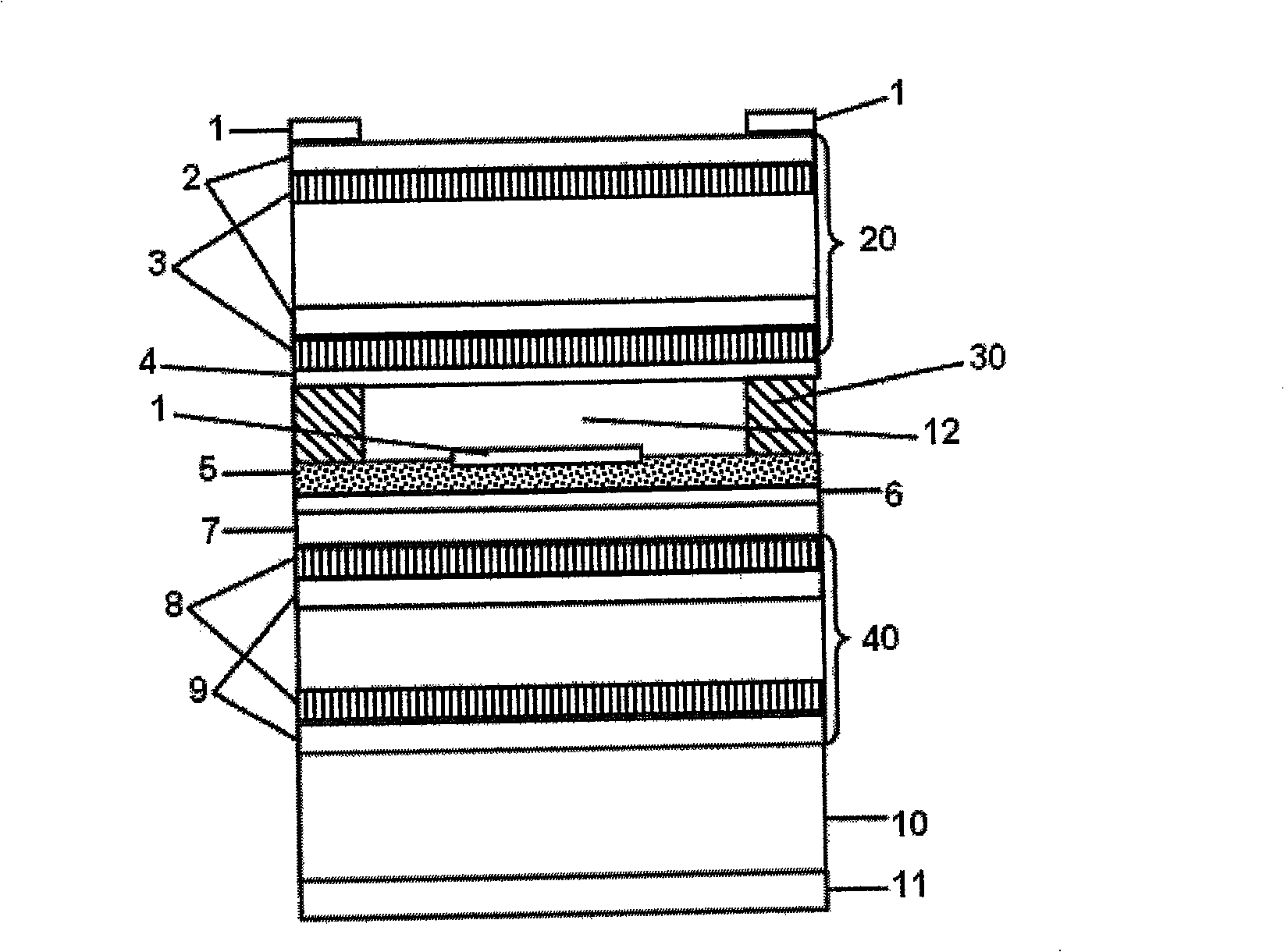
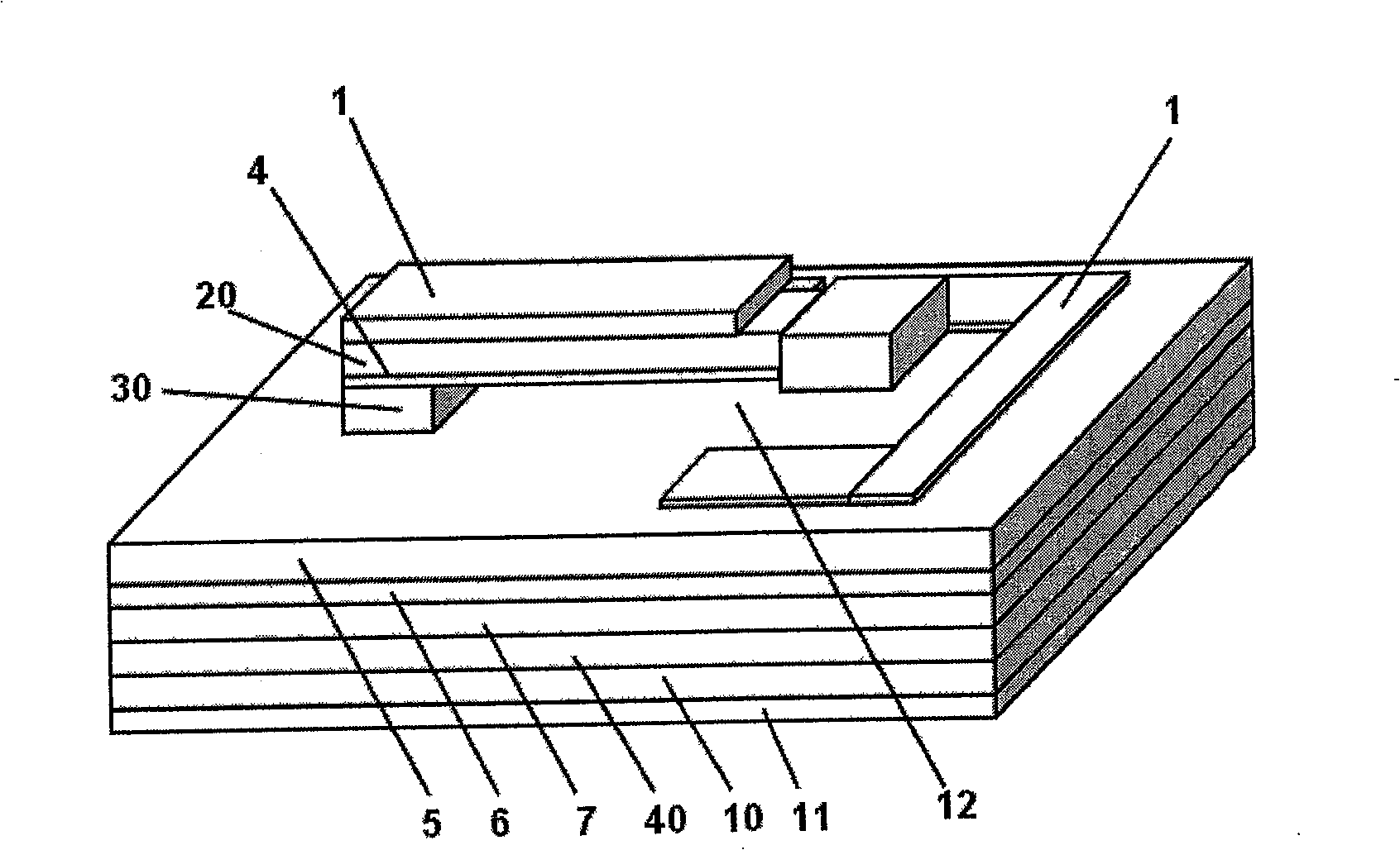
[0035] Step 1. Using metal organic chemical vapor deposition or molecular beam epitaxy system to sequentially epitaxially grow 26 pairs of n-type aluminum gallium arsenide layer 9 and n-type gallium arsenide layer 8 on n-gallium arsenide substrate 10, GaInAs / GaAs quantum well structure active region 7, oxidation confinement layer AlGaAs layer 6, p-type ohmic contact layer 5;
[0036] Step 2, using metal organic chemical vapor deposition or molecular beam epitaxy system to epitaxially grow the sacrificial layer AlGaAs layer on the p-type ohmic contact layer 5, and continue to epitaxially grow the gallium indium phosphorus etching stop layer 4 and 23 on the gallium arsenide layer 2 and a distributed feedback Bragg reflector 20 reflectors on the AlGaAs layer 3;
[0037] Step 3, using a method of combining photolithography and selective wet etching, selectively etching the upper distributed feedback Bragg reflector 20 reflectors to prepare a three-dimensional contour figure of th...
Embodiment 2
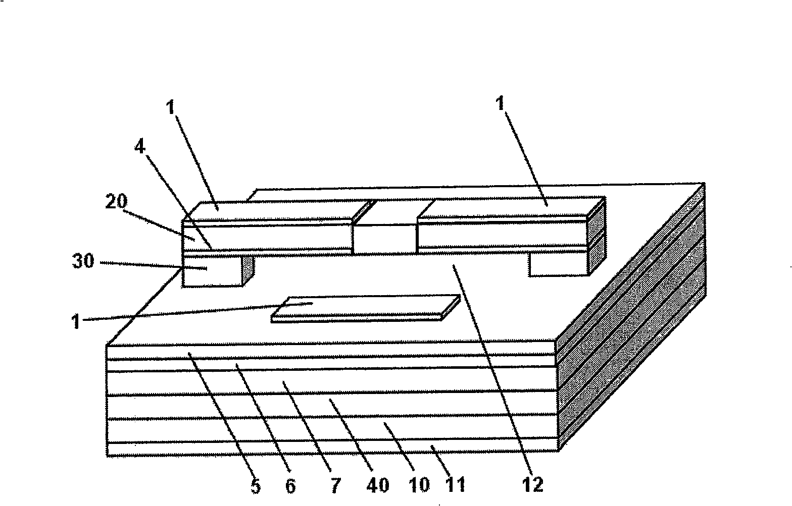
[0046] Step 1. Using metal organic chemical vapor deposition or molecular beam epitaxy system to sequentially epitaxially grow 26 pairs of n-type aluminum gallium arsenide layer 9 and n-type gallium arsenide layer 8 on n-gallium arsenide substrate 10, GaInAs / GaAs quantum well structure active region 7, oxidation confinement layer AlGaAs layer 6, p-type ohmic contact layer 5;
[0047] Step 2: Prepare a polyimide film on the p-type ohmic contact layer 5 by photolithography, and then continue to grow 10 pairs of Si by plasma chemical vapor deposition. 3 N 4 / SiO 2 The upper distributed feedback Bragg reflector mirror, the thickness of each pair of distributed feedback Bragg reflectors is 1 / 2 of the lasing wavelength;
[0048] Step 3, using a combination of photolithography and plasma etching, the upper distributed feedback Bragg mirror 20 is selectively etched to prepare a three-dimensional profile of the cantilever beam;
[0049] Step 4, performing secondary photolithography...
PUM
 Abstract
Description
Claims
Application Information
 - R&D
- Intellectual Property
- Life Sciences
- Materials
- Tech Scout
- Unparalleled Data Quality
- Higher Quality Content
- 60% Fewer Hallucinations
Browse by: Latest US Patents, China's latest patents, Technical Efficacy Thesaurus, Application Domain, Technology Topic, Popular Technical Reports.
© 2025 PatSnap. All rights reserved.Legal|Privacy policy|Modern Slavery Act Transparency Statement|Sitemap|About US| Contact US: help@patsnap.com


