Plasma etching method
A technology of plasma etching and plasmaization, which is applied in the field of ion etching, can solve the problems that it is difficult to control the shape of the groove, the depth-to-diameter ratio of the groove shape cannot be satisfied at the same time, and the groove side wall is concave-convex, etc., and achieves the effect of high practical value
- Summary
- Abstract
- Description
- Claims
- Application Information
AI Technical Summary
Problems solved by technology
Method used
Image
Examples
no. 1 Embodiment approach
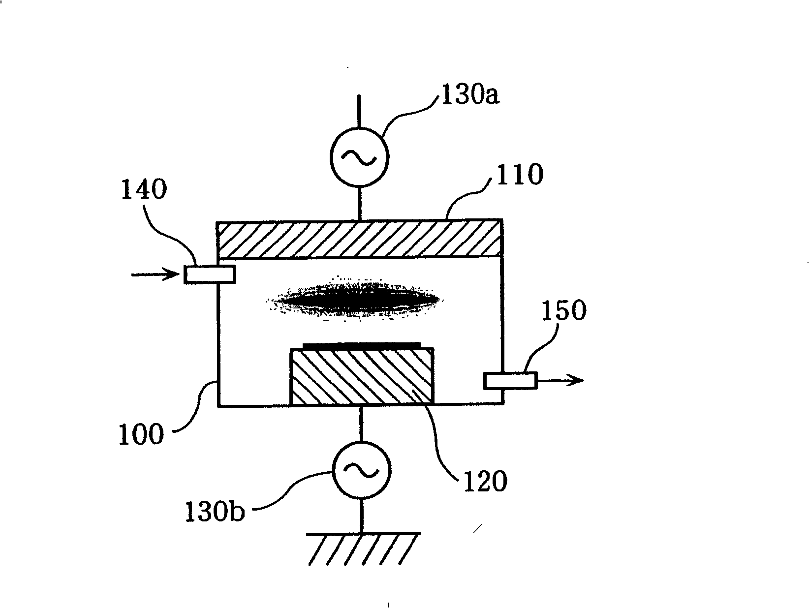
[0073] figure 1 It shows the structure of the plasma etching apparatus of 1st Embodiment.
[0074] Plasma etching device is a kind of etching device such as ICP (Inductively Coupled Plasma) type, has following equipment: vacuum etching processing chamber 100, upper electrode 110 and lower electrode 120 in etching processing chamber 100, high-frequency power supply 130a, 130b and gas introduction port 140 and exhaust port 150.
[0075] The etching chamber 100 is an etching chamber, and its inner wall is made of an insulating material such as quartz, alumina, an aluminum base material treated with an alumina film (corrosion-resistant treatment), or yttrium oxide.
[0076] The high-frequency power sources 130a and 130b supply high-frequency power of, for example, 13.56 MHz.
[0077] The gas inlet 140 supplies gas to the etching chamber 100 .
[0078] The exhaust port 150 exhausts gas within the etching process chamber 100 .
[0079] Next, a method of trenching a silicon subs...
no. 2 Embodiment approach
[0089] In the plasma etching apparatus of the above-mentioned first embodiment, as the etching gas, a gas containing SF should be used. 6 Gas, O 2 For the mixed gas of gas and rare gas, high-frequency power of, for example, 13.56 MHz should be applied to the mixed gas. However, as an etching gas, even if it does not contain O 2 Mixed gas of gas, which contains SF 6 The same effect can also be obtained by applying a high-frequency power of 27 MHz or higher to a mixed gas of a fluorine compound gas such as gas and a rare gas.
[0090] Therefore, in the plasma etching apparatus of the second embodiment, as an etching gas, a gas containing SF 6 Fluorine compound gas such as gas and a mixed gas of a rare gas, and a high-frequency power of 27 MHz or more is applied to the mixed gas. Next, a description will be given centering on differences from the first embodiment.
[0091] Figure 4 It shows the structure of the plasma etching apparatus of 2nd Embodiment.
[0092] The plas...
no. 3 Embodiment approach
[0103] In the plasma etching apparatus of the above-mentioned first embodiment, as the etching gas, a gas containing SF should be used. 6 Gas, O 2 Gases and mixtures of rare gases. However, as an etching gas, even if the use contains SF 6 The mixed gas of fluorine compound gas, polymer forming gas, and rare gas can also achieve the same effect, and can suppress the etching of silicon substrates with insulating barrier layers under SOI (Silicon On Insulator) substrates, etc. When the lateral etching occurs.
[0104] That is: in the case of the plasma etching apparatus of the first embodiment, by O 2 Reaction products formed from the reaction with silicon protect the sidewalls of the trench. Therefore, on an SOI substrate, etc., once the barrier layer is exposed due to etching, the generation of reaction products will stop and the sidewall of the trench can no longer be protected. On the silicon substrate 910 near the barrier layer 920, such as Figure 6 The notch 900 is sh...
PUM
 Abstract
Description
Claims
Application Information
 - R&D Engineer
- R&D Manager
- IP Professional
- Industry Leading Data Capabilities
- Powerful AI technology
- Patent DNA Extraction
Browse by: Latest US Patents, China's latest patents, Technical Efficacy Thesaurus, Application Domain, Technology Topic, Popular Technical Reports.
© 2024 PatSnap. All rights reserved.Legal|Privacy policy|Modern Slavery Act Transparency Statement|Sitemap|About US| Contact US: help@patsnap.com


