Power and signal line bussing method for memory devices

a memory device and signal line technology, applied in the field of power and signal line bussing method for high density and high speed memory devices, can solve the problems of large signal delay, conventional bussing arrangement, and ineffective reduction of the frequency response of the peripheral circuit 4, so as to reduce the noise generated by the chip, fast access time, and the effect of not increasing the size of the chip

Inactive Publication Date: 2000-01-11
SAMSUNG ELECTRONICS CO LTD
View PDF6 Cites 2 Cited by
  • Summary
  • Abstract
  • Description
  • Claims
  • Application Information

AI Technical Summary

Benefits of technology

Another object of the present invention is to reduce chip noise generated in high speed memory devices without increasing chip size.
Still another object of the present invention is to provide a fast access time by eliminating excess path distance.
Yet another object is to provide an additional insulative layer above memory cells to reduce soft error.

Problems solved by technology

However, employing a single power line 3a to couple power to peripheral circuitry 4 does not effectively reduce noise.
However, signal line bussing according to this arrangement results in large signal delays because signals from pad 6 or internal circuit 6' must propagate the extra distance required to circumvent memory cell arrays 2.
A final disadvantage of conventional bussing arrangement arises inherently from the design.
Yet, even with the passivation and insulation layers, radiation generated from the package material layer penetrates the memory cells and causes a soft (or operation) error.

Method used


Image

  • Power and signal line bussing method for memory devices
  • Power and signal line bussing method for memory devices
  • Power and signal line bussing method for memory devices

Examples


Embodiment Construction

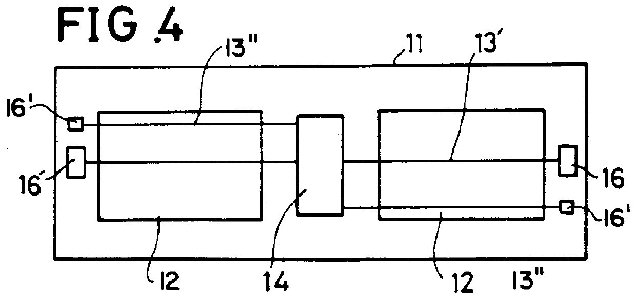
FIG. 3 shows a power line bussing arrangement according to the present invention. Chip 11 comprises two memory cell arrays 12 centered around peripheral circuitry 14. Power lines 13a, formed above memory cell arrays 12 and peripheral circuitry 14, supplies power from Vcc pad 15 to peripheral circuitry 14. Ground lines 13b, formed above memory cell arrays 12 and peripheral circuitry 14, connects peripheral circuitry 14 to GND pad 15'. Both power lines 13a and ground lines 13b are separated parallel lines traversing end-to-end chip 11. All power lines 13a are connected to Vcc pad 15 and all ground lines 13b are connected to GND pad 15'. Ground lines 13b and power lines 13a are formed in an adjacent alternating pattern such that a power line 13a is positioned adjacent to ground line 13b, which is positioned adjacent another power line 13a, and so on.

Accordingly, Vcc power is supplied through Vcc pad 15 and power lines 13 to each circuit in the peripheral circuitry 14. By coupling a pow...


PUM


Abstract

A memory cell device having circuitry located between memory cell arrays comprises power and ground lines to the circuitry formed directly above the memory cell arrays. The power and ground lines are parallel and positioned in an adjacent alternating pattern such that a power line is positioned adjacent a ground line, which is positioned adjacent another power line and so on. Signal lines carrying signals to and from the circuitry are also formed directly above memory cell arrays.

Description

BACKGROUND OF THE INVENTION1. Field of the InventionThe present invention relates to a power and signal line bussing method for high density and high speed memory devices.2. Description of the Prior ArtA conventional power line bussing method is shown in FIG. 1. Chip 1 has two memory cell arrays 2 centered around peripheral circuitry 4, which comprises multiple logic circuits. Power line 3a supplies power from Vcc pad to peripheral circuitry 4. Power line 3a runs from Vcc pad 5, around memory cell array 2, to peripheral circuitry 4. Ground line 3b electrically connects peripheral circuitry 4 with GND pad 5'. Ground line 3b runs from GND pad 5', around memory cell array 2, to peripheral circuitry 4.However, employing a single power line 3a to couple power to peripheral circuitry 4 does not effectively reduce noise. To best reduce noise, a power line should be coupled independently to each circuit in peripheral circuitry 4. Yet, separating power line 3a further would increase the chip...

Claims


Application Information

Patent Timeline
Patent Type & Authority Patents(United States)
IPC IPC(8): G11C5/14G11C5/02G11C11/41G11C11/34G11C11/401H01L21/822H01L27/04H01L27/10
CPCG11C5/025G11C5/14G11C11/34
Inventor HWANG, SANG KIJUNG, TAE SUNGCHOI, KYU HYUN
Owner SAMSUNG ELECTRONICS CO LTD
Why Eureka
Try Eureka