Memory cell including transistor and capacitor

a memory cell and capacitor technology, applied in semiconductor devices, digital storage, instruments, etc., can solve the problems of power supply voltage, standby current, memory size, power supply voltage, etc., and achieve the effect of reducing standby current, reducing size, and lowering power supply voltag

Active Publication Date: 2016-08-02
SEMICON ENERGY LAB CO LTD
View PDF16 Cites 0 Cited by
  • Summary
  • Abstract
  • Description
  • Claims
  • Application Information

AI Technical Summary

Benefits of technology

[0008]In principle, the minimum value of power supply voltage is the sum of the absolute value of the threshold voltage of a p-channel transistor and the absolute value of the threshold voltage of an n-channel transistor; thus, lowering the voltage is difficult. In addition, as a transistor is scaled down, variations in the threshold voltage of the transistor become larger. Furthermore, as the variations in the threshold voltage of the transistor become larger, a static noise margin (SNM) becomes smaller. Thus, when the transistor is scaled down, lowering the voltage is more difficult.
[0011]It is an object of one embodiment of the present invention to lower power supply voltage. Alternatively, it is an object of one embodiment of the present invention to reduce standby current. Alternatively, it is an object of one embodiment of the present invention to reduce size. Alternatively, it is an object of one embodiment of the present invention to provide a novel structure or configuration.
[0024]One embodiment of the present invention can lower power supply voltage. Alternatively, one embodiment of the present invention can reduce standby current. Alternatively, one embodiment of the present invention can reduce size. Alternatively, one embodiment of the present invention can provide a novel structure or configuration.

Problems solved by technology

In accordance with process scaling, a memory including a CMOS circuit, such as an SRAM, has problems of power supply voltage, standby current, and memory size.
In principle, the minimum value of power supply voltage is the sum of the absolute value of the threshold voltage of a p-channel transistor and the absolute value of the threshold voltage of an n-channel transistor; thus, lowering the voltage is difficult.
Thus, when the transistor is scaled down, lowering the voltage is more difficult.
However, as the transistor is scaled down, the proportion of gate-induced drain leakage (GIDL), gate tunnel leakage, junction leakage, and the like in the standby current becomes higher.
However, as described above, lowering the voltage is difficult.

Method used


Image

  • Memory cell including transistor and capacitor
  • Memory cell including transistor and capacitor
  • Memory cell including transistor and capacitor

Examples


embodiment 1

[0075]In this embodiment, a memory cell and a semiconductor storage device that can include the memory cell are described. Note that the memory cell is also referred to as a semiconductor device. In addition, the semiconductor storage device is also referred to as a semiconductor device.

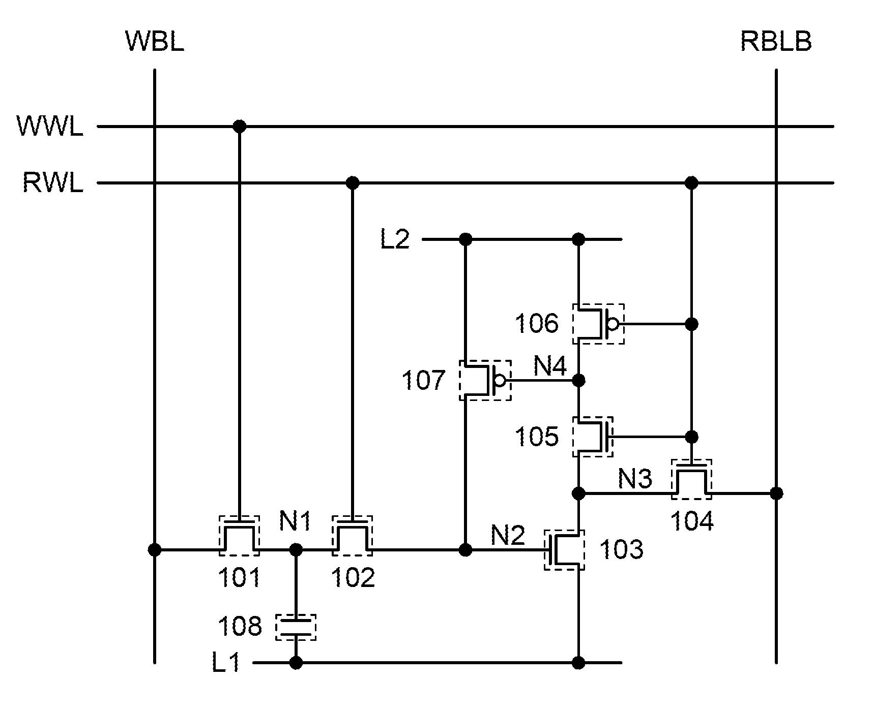
[0076]First, a memory cell structure is described with reference to a circuit diagram of a memory cell in FIG. 1.

[0077]The memory cell in FIG. 1 includes transistors 101 to 107 and a capacitor 108.

[0078]The conductivity types of the transistors 101 to 107 are not limited as long as the following operation can be performed. Note that for convenience, the transistors 101 to 105 are n-channel transistors, and the transistors 106 and 107 are p-channel transistors.

[0079]A first terminal of the transistor 101 is connected to a wiring WBL. A gate of the transistor 101 is connected to a wiring WWL. A first terminal of the transistor 102 is connected to a second terminal of the transistor 101. A gate of the t...

embodiment 2

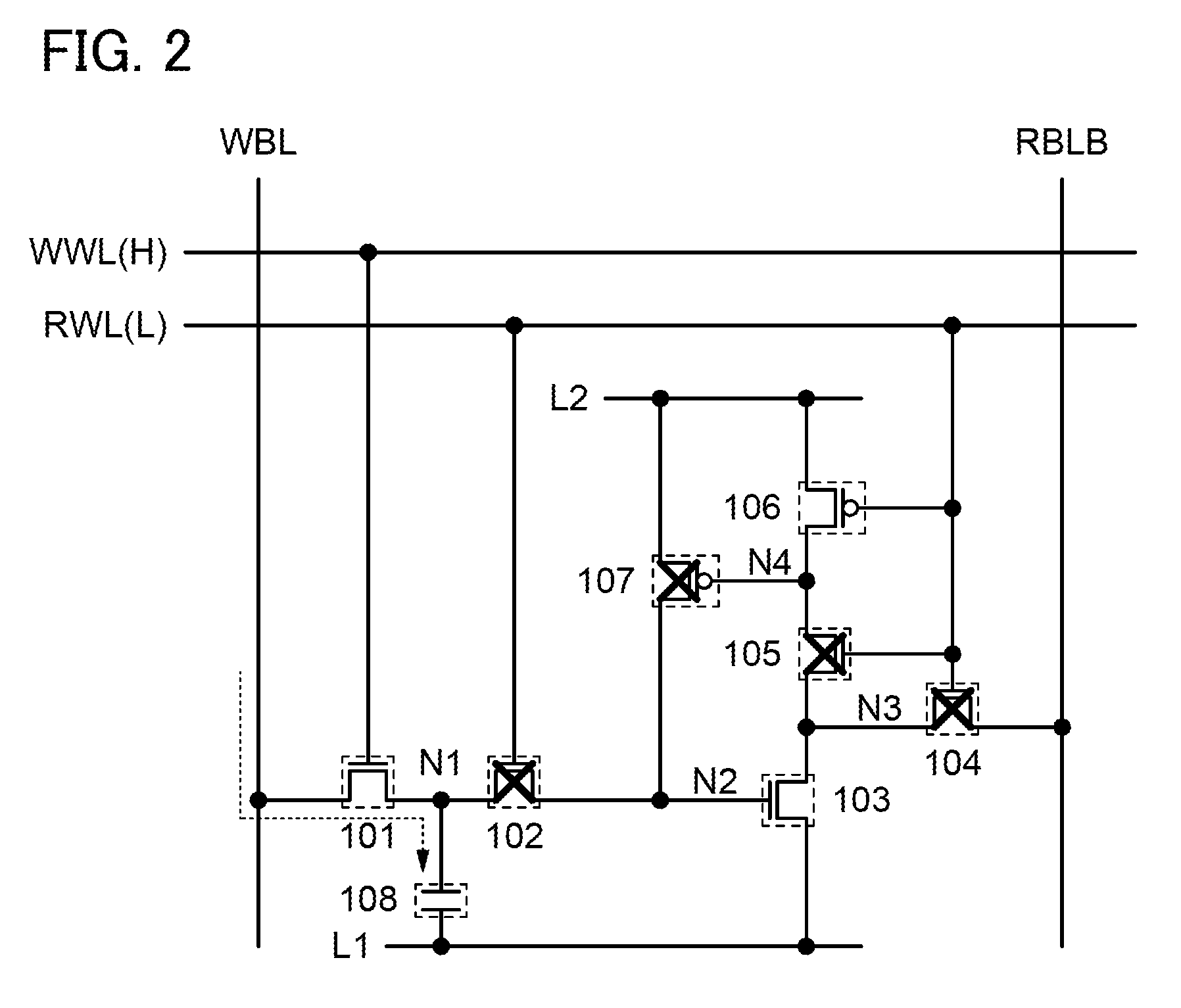
[0157]In this embodiment, a memory cell different from the memory cell in Embodiment 1 is described. Note that components in common with those in Embodiment 1 are denoted by the same reference numerals, and description thereof is omitted. In addition, the description of Embodiment 1 can be applied to a memory cell in this embodiment.

[0158]First, a memory cell in FIG. 10 differs from the memory cell in FIG. 1 in that a transistor 109 whose first terminal is connected to the wiring L1, whose second terminal is connected to the node N2, and whose gate is connected to the wiring WBL is provided. The on or off state of the transistor 109 is controlled by the signal VWBL.

[0159]An operation example of the memory cell in FIG. 10 is described. Before the start time of a data read period, i.e., in a data write period or a data retention period, to turn on the transistor 109, the signal VWBL is set at a potential (e.g., high level) at which the transistor 109 is turned on. When the transistor ...

embodiment 3

[0220]In this embodiment, a semiconductor device is described. The semiconductor device in this embodiment can be applied to the RBLB driver circuit 240 in FIG. 6.

[0221]First, the structure of the semiconductor device is described with reference to a circuit diagram of a semiconductor device in FIG. 26.

[0222]The semiconductor device in FIG. 26 includes a precharge circuit 300, a sense amplifier 310, and a data latch circuit 320. The precharge circuit 300 is connected to the wiring RBLB, a wiring RBLA, a wiring RPC, and a wiring L3. The sense amplifier 310 is connected to the wiring RBLB, the wiring RBLA, a wiring SA, a wiring L4, and a wiring L5. The data latch circuit 320 is connected to the wiring RBLB, the wiring RBLA, and a wiring RBL.

[0223]The signal VRBLB is input to the wiring RBLB. The signal VRBLB is controlled by data read from a memory cell.

[0224]A signal VRPC is input to the wiring RPC. The signal VRPC controls the precharge circuit 300 and has two states (active and ina...


PUM


Abstract

A semiconductor storage device capable of performing low-voltage operation, reducing standby current, and decreasing memory size is provided. The semiconductor storage device is a semiconductor device including first to fourth transistors and a capacitor. The first transistor has a function of supplying a first signal to the capacitor. The capacitor has a function of accumulating electric charge based on the first signal. The second transistor has a function of supplying the electric charge based on the first signal to a gate of the third transistor. The third transistor has a function of outputting a first potential to a wiring and a function of supplying the first potential to a gate of the fourth transistor. The fourth transistor has a function of supplying a second potential to the capacitor through the second transistor.

Description

BACKGROUND OF THE INVENTION[0001]1. Field of the Invention[0002]One embodiment of the present invention relates to a semiconductor device, a method for driving the semiconductor device, a semiconductor storage device, a method for driving the semiconductor storage device, a memory cell, or a method for driving the memory cell.[0003]Note that one embodiment of the present invention is not limited to the above technical field. The technical field of the invention disclosed in this specification and the like relates to an object, a method, or a manufacturing method. In addition, the present invention relates to a process, a machine, manufacture, or a composition of matter. Specifically, examples of the technical field of one embodiment of the present invention disclosed in this specification include a semiconductor device, a display device, a light-emitting device, a power storage device, a storage device, a method for driving any of them, and a method for manufacturing any of them.[00...

Claims


Application Information

Patent Timeline
Patent Type & Authority Patents(United States)
IPC IPC(8): G11C5/06H01L27/11G11C7/10G11C11/24
CPCH01L27/1116G11C5/063G11C8/14G11C8/16G11C7/1075G11C11/24G11C5/06G11C2207/2209H10B10/18
Inventor MAEHASHI, YUKIO
Owner SEMICON ENERGY LAB CO LTD
Why Eureka
Try Eureka