Spin injector device comprising a protection layer at the centre thereof

a technology of injector device and protection layer, which is applied in the field of electronic devices, can solve the problems of increasing the power and complexity of the device, reducing the performance of the device, or even disappearing, and reducing the transmission properties of the device, so as to promote the transfer of bias electrons, restrict or prevent oxidation and/or contamination of the face, and strong magnetic susceptibility

Active Publication Date: 2016-06-07
CENT NAT DE LA RECHERCHE SCI +1
View PDF9 Cites 1 Cited by
  • Summary
  • Abstract
  • Description
  • Claims
  • Application Information

AI Technical Summary

Benefits of technology

[0023]a) forming a protection layer on a face or a first face of a substrate, so as to restrict or prevent oxidation and / or contamination of said face by its environment, the face may be magnetic and electrically conductive, the protection layer may be diamagnetic or paramagnetic; preferably, the protection layer is paramagnetic and includes a strong magnetic susceptibility;
[0026]a) forming a metal protection layer on a face of a substrate, so as to restrict or prevent oxidation and / or contamination of said face by its environment, the face of the substrate being magnetic and electrically conductive, the protection layer being of a diamagnetic or paramagnetic nature;
[0029]The physics of the indirect exchange coupling, which is related to a mechanism allowing the projection of the magnetism from the substrate through a non-magnetic layer, herein the protection layer, operates essentially regardless of whether it is a metal or insulating or even semi-conducting protection layer. However, whereas the effect will be mainly oscillatory in the case of a metal layer, it will have a highly evanescent essential feature (that is exponentially decreasing) in the case of an insulating or semi-conducting layer. The exchange coupling achieved through the metal protection layer is thus much better in terms of amplitude (about 109 times higher) and intensity than through an insulating or semi-conducting layer, in particular considering layers having thicknesses higher than a monolayer (about 0.18 nm for a copper monolayer).
[0039]When the substrate and the protection layer are crystallised, it is possible to carefully select the thickness of the protection layer for, by virtue of the formation of a quantum well state within the protection layer, better projecting the density of spin biased states, from the first face of the substrate, to the opposite face of the protection layer, in contact with the upper layer to be spin biased.
[0047]The present invention thus also relates to a method for manufacturing a device including implementing a method for manufacturing a spin injector device according to the invention, and wherein the spin injector device may be connected to an intermediate device including a second protection layer provided on a second substrate, the second protection layer of the intermediate device may be provided against the substrate or the upper layer of the spin injector device. This configuration offers the advantage of being able to control the spin bias of the electrical current passing through the spin injector device, but also to pre-cease the spin referential frame of the upper layer to a frequency in the gigahertz range.
[0053]a protection layer on the face of the substrate, so as to restrict or prevent oxidation and / or contamination of said face by its environment, the protection layer may be of a low magnetic or diamagnetic or paramagnetic nature;

Problems solved by technology

Technological advances made in the semi-conductor industry allow to considerably reduce the dimensions of electronic devices, thus increasing their power and complexity.
But, the transmission properties may be quickly degraded when the interfaces include impurities and / or are oxidized.
In the field of inorganic spintronics, this can results in a decrease, or even a disappearance, of the spintronic performances of the device (Physical Review B79, 224405 (2009)).
This is one of the causes limiting the use of this kind of device at an industrial level.
Another drawback resides in the fact that the composition of the deposited organic layers should not contain elements likely to interact with the magnetic layer, so as to degrade its spintronic properties.
This is why, inter alia, spin injector devices, including an organic layer on a magnetic layer, are delicate to assemble, because of production environment requirements, and thereby restrain the type of molecule in the class of molecules vacuum sublimable.

Method used


Image

  • Spin injector device comprising a protection layer at the centre thereof
  • Spin injector device comprising a protection layer at the centre thereof
  • Spin injector device comprising a protection layer at the centre thereof

Examples


Embodiment Construction

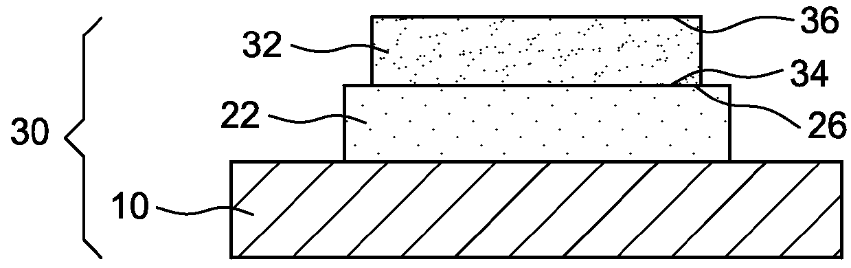
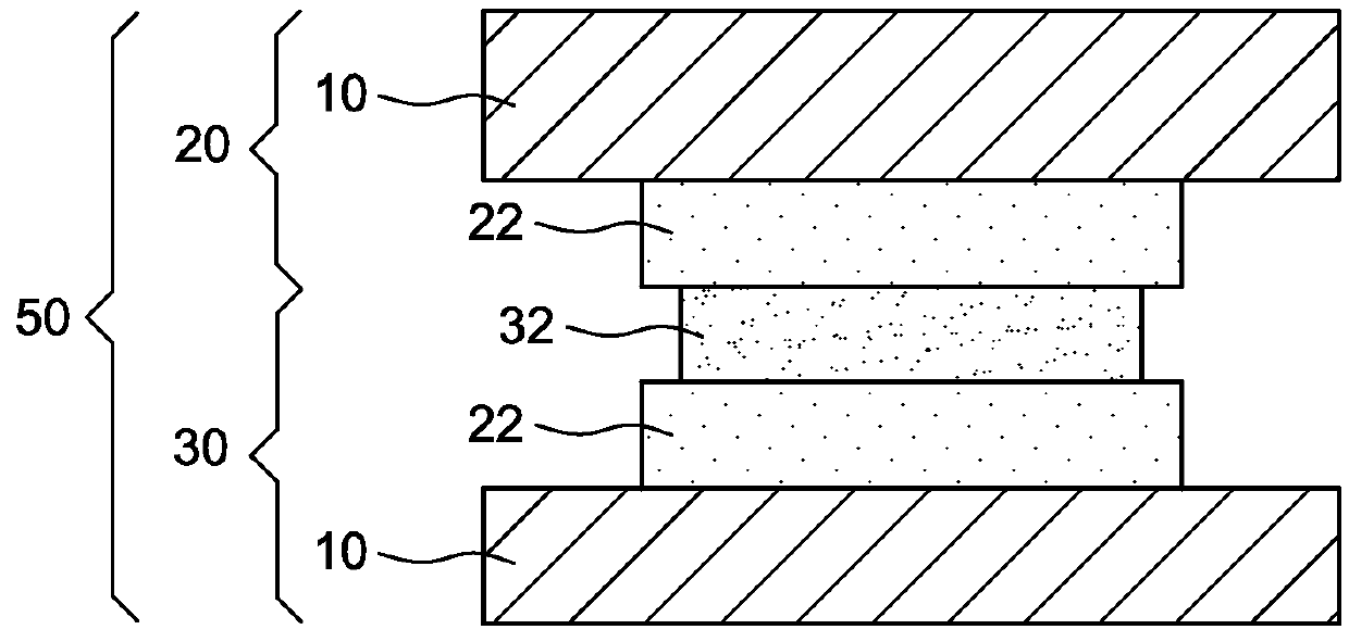
[0062]One of the purposes of the present application is to facilitate the manufacture of a device for injecting biased spins into a material, when connected to a current source. This type of device is also known as spin injector device.

[0063]A manufacturing method is facilitated when it is adaptable to industrial requirements, that is easy, and / or fast, and / or economical to implement, while being reproducible on a large scale.

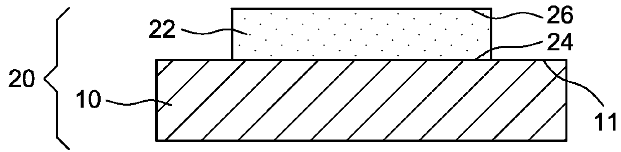
[0064]A spin injector device 30 includes a first material, called substrate 10, which is electrically conducting and has magnetic properties. A first face 11 of the substrate 10 is in contact with the outer environment and has ferromagnetic and / or ferrimagnetic and / or antiferromagnetic type magnetic properties (FIG. 1).

[0065]The first face 11 of the substrate can for example include or be based on oxide(s) and / or nitride(s), and / or carbide(s), or based on cobalt and / or iron, and / or nickel. The term “based on” defines a volume proportion equal to or higher than ...


PUM

PropertyMeasurementUnit
temperatureaaaaaaaaaa
thicknessesaaaaaaaaaa
exchange magnetic fieldaaaaaaaaaa

Abstract

A method for manufacturing a spin injector device, comprising the following steps of:a) forming a metal protection layer on a face of a substrate, so as to restrict or prevent oxidation and / or contamination of said face by its environment, the face being magnetic and electrically conductive, the protection layer being of a diamagnetic or paramagnetic nature;b) forming an upper layer onto the protection layer, able to promote a spin bias of electronics sates in the vicinity of the Fermi level of the interface between the protection layer and the upper layer according to an amplitude and a spin referential frame which are defined by the magnetism of the substrate and / or of the face of the substrate, the upper layer being an organic layer of which one or more molecular sites have, in contact with the protection layer, a paramagnetic moment.

Description

CROSS-REFERENCE TO RELATED PATENT APPLICATION[0001]The present application is a National Stage Application of International Application No. PCT / EP2013 / 057769 entitled “SPIN INJECTOR DEVICE COMPRISING A PROTECTION LAYER AT THE CENTRE THEREOF” filed Apr. 15, 2013, which claims benefit of priority to French patent Application No. 12 53569 filed on Apr. 18, 2012. Both of these applications are incorporated herein by reference in their entirety.TECHNICAL FIELD[0002]The present application relates to the technical field of electronics, more precisely that of spintronics. The invention particularly relates to a method of manufacturing a spin injector device, enabling electrons passing through it to be filtered, depending on the orientation of their spin.STATE OF PRIOR ART[0003]Technological advances made in the semi-conductor industry allow to considerably reduce the dimensions of electronic devices, thus increasing their power and complexity. Nowadays, manufacturing these devices in the a...

Claims


Application Information

Patent Timeline
Patent Type & Authority Patents(United States)
IPC IPC(8): H01L43/12H01F41/32H01F10/00H01F10/32H01L43/10
CPCH01L43/12H01F10/005H01F10/3254H01F41/32H01L43/10H10N50/85H10N50/01
Inventor BOWEN, MARTINALOUANI, MEBAREKBOUKARI, SAMYBEAUREPAIRE, ERICWEBER, WOLFGANGSCHEURER, FABRICEJOLY, LOIC
Owner CENT NAT DE LA RECHERCHE SCI
Why Eureka
Try Eureka