
Method and system for lithography process-window-maximixing optical proximity correction

a technology of lithography and window, applied in the field of method and system of lithography process window, can solve the problems of difficult to reproduce a pattern on the wafer, large cost of making high-end mask sets, and general inability to apply opc, etc., and achieve the effect of maximizing the process window

Active Publication Date: 2016-06-07
ASML NETHERLANDS BV
View PDF45 Cites 7 Cited by
  • Summary
  • Abstract
  • Description
  • Claims
  • Application Information

AI Technical Summary

Benefits of technology

This approach significantly reduces computation time while maximizing the process window, allowing for more efficient OPC and enabling applications such as model calibration, yield estimation, and process control corrections.

Problems solved by technology

These rules are set by processing and design limitations.
In general, the smaller k1, the more difficult it becomes to reproduce a pattern on the wafer that resembles the shape and dimensions planned by a circuit designer in order to achieve particular electrical functionality and performance.
However, applying OPC is generally not an ‘exact science’, but an empirical, iterative process that does not always resolve all possible weaknesses on a layout.
This is driven by the enormous cost of making high-end mask sets, which run in the multi-million dollar range, as well as by the impact on turn-around time by reworking or repairing actual masks once they have been manufactured.
While full-chip numerical simulation of the lithographic patterning process has been demonstrated at a single process condition, typically best focus and best exposure dose or best ‘nominal’ condition, it is well known that manufacturability of a design requires sufficient tolerance of pattern fidelity against small variations in process conditions that are unavoidable during actual manufacturing.
However, such an increase in the computational time is prohibitive when attempting to validate and / or design a given target circuit.

Method used


Image

  • Method and system for lithography process-window-maximixing optical proximity correction
  • Method and system for lithography process-window-maximixing optical proximity correction
  • Method and system for lithography process-window-maximixing optical proximity correction

Examples


Embodiment Construction

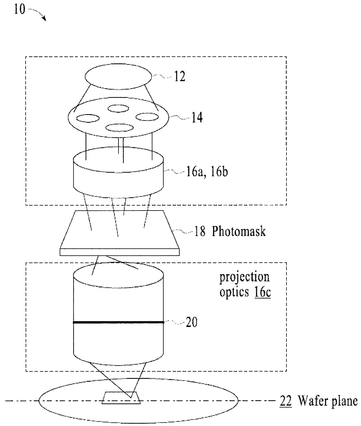
[0046]The present invention will now be described in detail with reference to the drawings, which are provided as illustrative examples of the invention so as to enable those skilled in the art to practice the invention. Notably, the figures and examples below are not meant to limit the scope of the present invention to a single embodiment, but other embodiments are possible by way of interchange of some or all of the described or illustrated elements. Moreover, where certain elements of the present invention can be partially or fully implemented using known components, only those portions of such known components that are necessary for an understanding of the present invention will be described, and detailed descriptions of other portions of such known components will be omitted so as not to obscure the invention. Embodiments described as being implemented in software should not be limited thereto, but can include embodiments implemented in hardware, or combinations of software and...


PUM

PropertyMeasurementUnit
wavelengthaaaaaaaaaa

Abstract

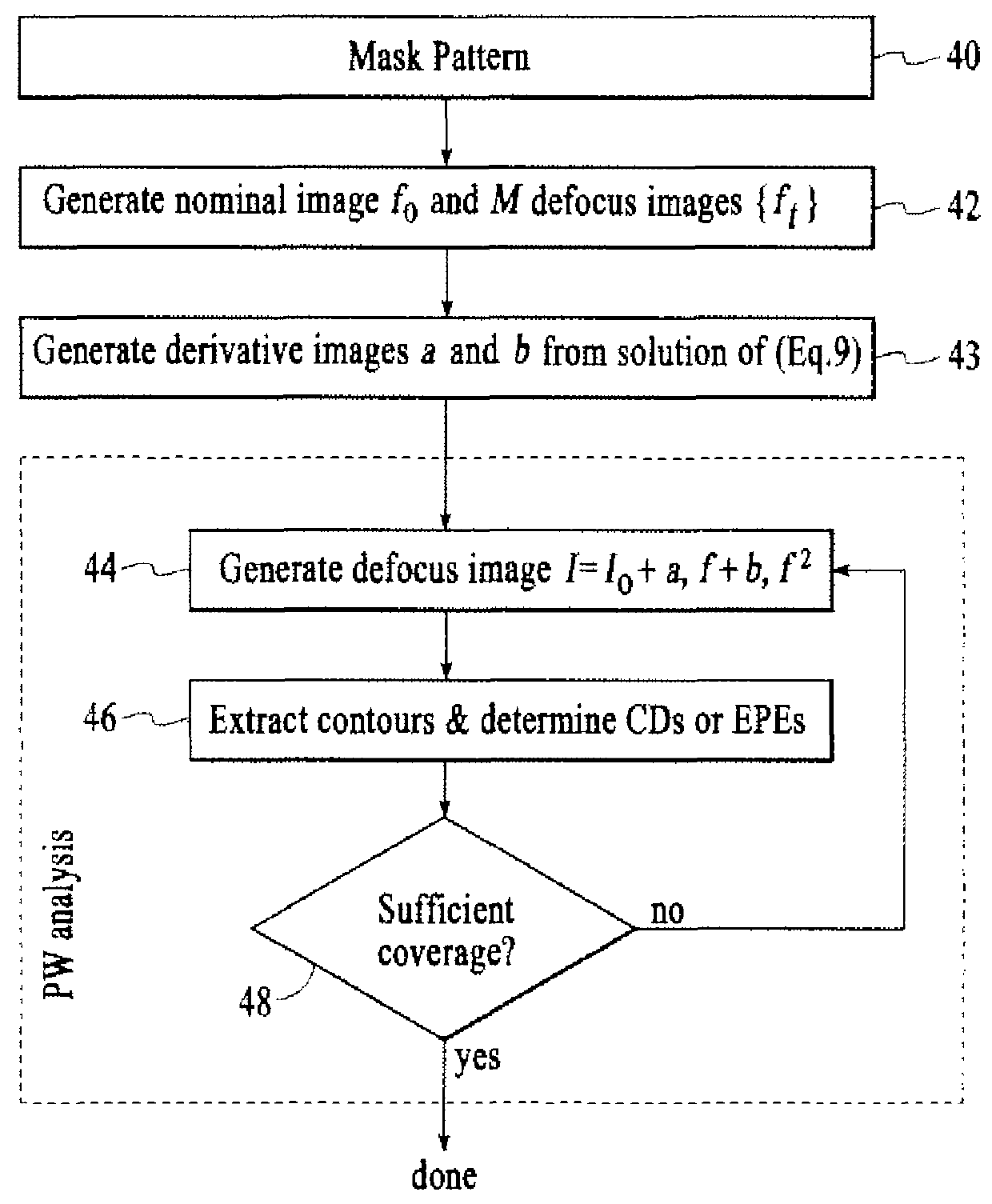
The present invention relates to an efficient OPC method of increasing imaging performance of a lithographic process utilized to image a target design having a plurality of features. The method includes the steps of determining a function for generating a simulated image, where the function accounts for process variations associated with the lithographic process; and optimizing target gray level for each evaluation point in each OPC iteration based on this function. In one given embodiment, the function is approximated as a polynomial function of focus and exposure, R(ε, f )=P0+f2·Pb with a threshold of T+Vε for contours, where P0 represents image intensity at nominal focus, f represents the defocus value relative to the nominal focus, ε represents the exposure change, V represents the scaling of exposure change, and parameter “Pb” represents second order derivative images. In another given embodiment, the analytical optimal gray level is given for best focus with the assumption that the probability distribution of focus and exposure variation is Gaussian.

Description

CROSS-REFERENCE TO RELATED APPLICATIONS[0001]The present application claims priority to U.S. Prov. Appln. No. 61 / 138,865, filed on Dec. 18, 2008, the contents of which are incorporated herein by reference in their entirety.FIELD OF THE INVENTION[0002]The present invention relates generally to a method and program product for performing simulation and the optical proximity correction of the imaging results associated with a lithography process, and more specifically to a computationally efficient optical proximity correction (OPC) method of optimizing imaging performance of a lithographic apparatus that accounts for parameter variations over a process window.BACKGROUND OF THE INVENTION[0003]Lithographic apparatus can be used, for example, in the manufacture of integrated circuits (ICs). In such a case, the mask may contain a circuit pattern corresponding to an individual layer of the IC, and this pattern can be imaged onto a target portion (e.g. comprising one or more dies) on a subs...

Claims


Application Information

Patent Timeline
Patent Type & Authority Patents(United States)
IPC IPC(8): G06F17/50G03F7/20G03F1/00G03F1/36
CPCG03F7/70441G03F1/144G03F1/36G03F7/705G06F30/398G06F2119/18
Inventor YE, JUNCAO, YUFENG, HANYING
Owner ASML NETHERLANDS BV
Learn More