Laser conversion of high purity silicon powder to densified granular forms
a technology of densification granular form and silicon powder, which is applied in the direction of crystal growth process, silicon compounds, manufacturing tools, etc., can solve the problems of affecting the growth of the pv industry, significant shortfall of silicon feedstock material is still expected in the foreseeable future, and the by-product of silicon powder is presently very difficult to use, so as to achieve the effect of convenient manufacturing
- Summary
- Abstract
- Description
- Claims
- Application Information
AI Technical Summary
Benefits of technology
Problems solved by technology
Method used
Image
Examples
example 1
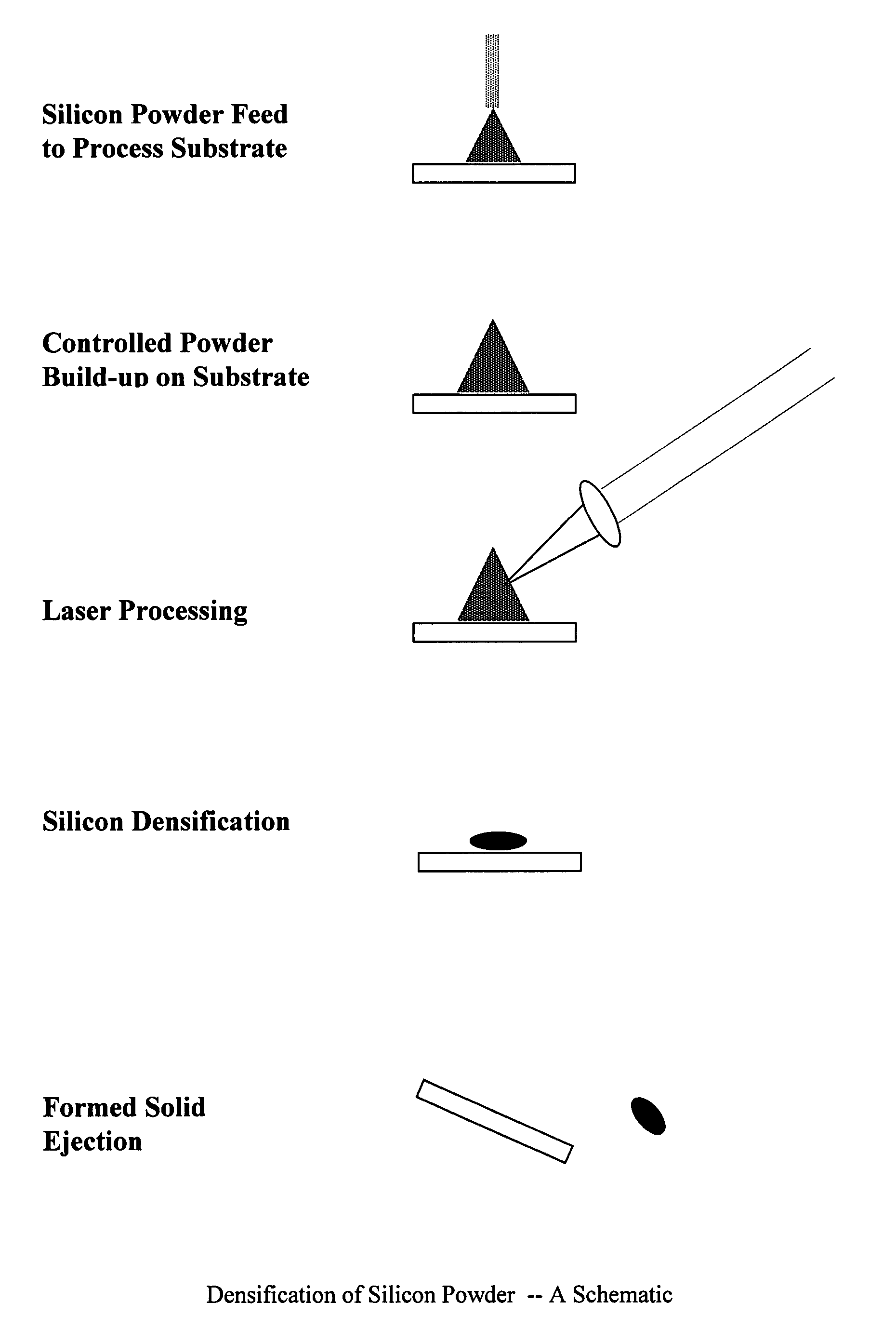
[0101]High purity silicon powder with particle size in the range of 0.1 microns to 3 microns, and with mean diameter of 0.5 microns, was utilized. The bulk density of the powder was 0.3 grams per cubic centimeter, and which tapped to a density of 0.5 grams per cubic centimeter. A high purity semiconductor grade graphite block with drilled chambers approximately 5 mm in diameter and 6 mm in depth, and coated with boron nitride was used as the substrate. The silicon powder was placed in the holes and tamped. An IPG Photonics YLR-1700 Yb:YAG laser was used. The laser setup utilized a focus of 150 mm, 60 mm collimator and 100 microns diameter fiber with defocused beam just below the focal plane. An argon cover gas was used around the process area to prevent oxidation. When using a laser power of 85 W CW, and with an approximate beam spot size of 4 mm to 5 mm, for 5 to 6 seconds, the silicon charge melted, coalesced and formed a granule in the bottom of the chamber. The granule sizes var...
example 2
[0104]The high purity silicon powder of Example 1, and a second supply of high purity silicon powder with a particle size in the range of 0.1 microns to 20 microns, and a mean diameter of 1 micron, was used. The bulk density of the powder of the second supply was 0.4 grams per cubic centimeter and the tap density was >0.5 grams per cubic centimeter. The substrate was a high purity h-boron nitride block having drilled conical chambers approximately 10 mm in diameter and 6 mm in depth, and with hemispherical bottoms which taper into approximately 5 mm in diameter, similar to the platform shown in FIG. 8. The silicon powder was distributed on the substrate and tamped into the chambers.
[0105]An IPG Photonics diode laser DLR-175 was utilized. The laser setup utilized a focus of 230 mm, 50 mm collimator and 400 microns diameter fiber, and the beam was defocused to provide a large spot of heat. Two off-axis inert argon gas jets, leading and trailing the laser beam, were used to protect the...
PUM
| Property | Measurement | Unit |
|---|---|---|
| diameter | aaaaa | aaaaa |
| diameter | aaaaa | aaaaa |
| mean particle size | aaaaa | aaaaa |
Abstract
Description
Claims
Application Information
 - R&D
- Intellectual Property
- Life Sciences
- Materials
- Tech Scout
- Unparalleled Data Quality
- Higher Quality Content
- 60% Fewer Hallucinations
Browse by: Latest US Patents, China's latest patents, Technical Efficacy Thesaurus, Application Domain, Technology Topic, Popular Technical Reports.
© 2025 PatSnap. All rights reserved.Legal|Privacy policy|Modern Slavery Act Transparency Statement|Sitemap|About US| Contact US: help@patsnap.com


