Sputtering target and process for producing same
a technology of sputtering target and process, applied in the field of sputtering target, can solve the problems of defective products, particle and nodules generation, and such defects in sputtering, and achieve the effects of superior surface characteristics, preventing or inhibiting the generation of particles and nodules during sputtering
- Summary
- Abstract
- Description
- Claims
- Application Information
AI Technical Summary
Benefits of technology
Problems solved by technology
Method used
Image
Examples
example 1
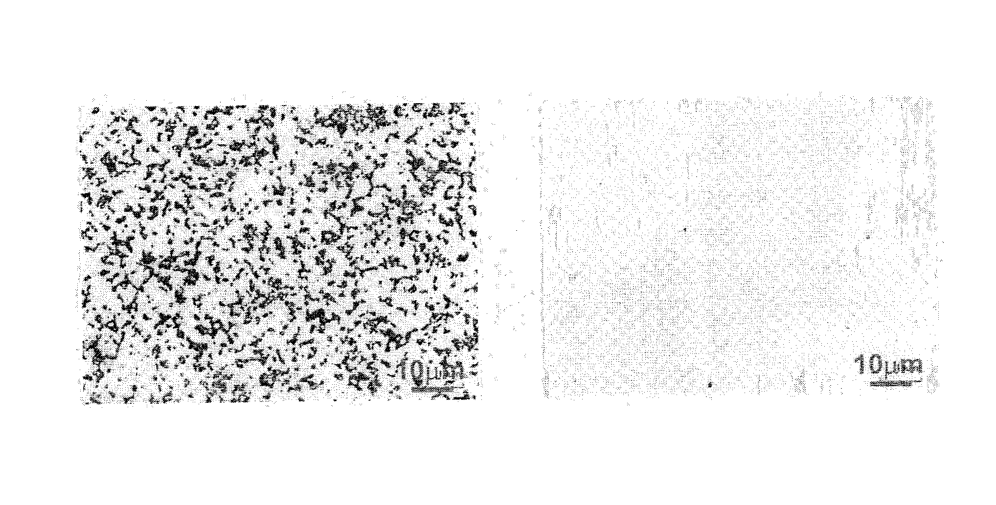
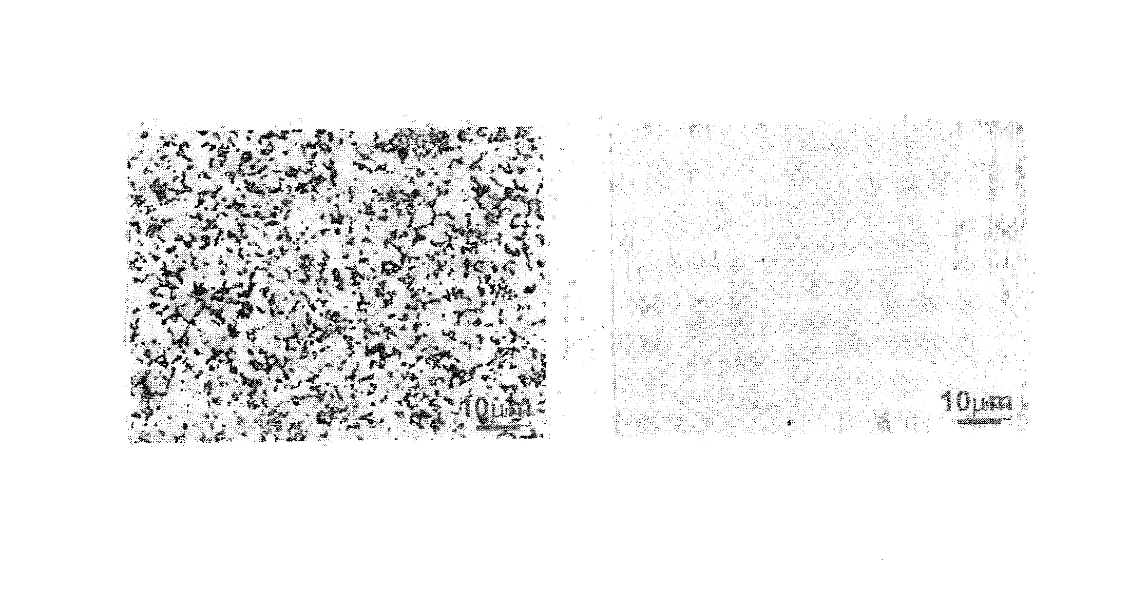
[0047]Co powder, Cr powder, Pt powder, and SiO2 powder were used as the raw material, and a target raw material was obtained based on the production conditions of hot pressing and HIP. The volume ratio of SiO2 without ductility in this target was 25%, and the average grain size of the SiO2 grains was 2 μm. The major component of the matrix phase was a uniform Co—Cr—Pt alloy.
[0048]After performing primary processing of cutting using a lathe to finalize a target shape, grinding processing was additionally performed, and the processes of wet secondary polishing including wet primary polishing based on pure water drop→alumina polishing agent drop were performed to adjust the surface and obtain a target.
[0049]The average surface roughness of the target in which the surface roughness was adjusted as described above; specifically, the measurement results of the center-line average surface roughness Ra, the ten-point average roughness Rz, the distance between local peaks (roughness motif) A...
example 2
[0055]Other than achieving Ra of 0.256 μm, Rz of 1.234 μm, AR of 118.76 μm, and AW of 1530.50 μm in the processes of wet secondary polishing, a cobalt coated target was produced based on the same production conditions as Example 1, and a sputtered film was formed on a substrate in an Ar 1.5 Pa atmosphere under the DC sputtering condition of 30 w / cm2.
[0056]When observing the particles that were generated during the sputtering, the size of the particles was approximately 1 μm×1 μm (“long diameter×short diameter”; hereinafter the same), and there was hardly any difference in comparison to the grain size of oxides of approximately 1 μm×1 μm.
[0057]The results are similarly shown in Table 1. In addition, the number of defectives (defectives / mm2) caused by the particles was reduced to 2.2.
[0058]Even if the renter-line average surface roughness Ra is outside the range of 0.1 μm or less, the ten-point average roughness Rz is outside the range of 0.4 μm or less, distance between local peaks (...
PUM
| Property | Measurement | Unit |
|---|---|---|
| length | aaaaa | aaaaa |
| roughness | aaaaa | aaaaa |
| roughness | aaaaa | aaaaa |
Abstract
Description
Claims
Application Information
 - R&D
- Intellectual Property
- Life Sciences
- Materials
- Tech Scout
- Unparalleled Data Quality
- Higher Quality Content
- 60% Fewer Hallucinations
Browse by: Latest US Patents, China's latest patents, Technical Efficacy Thesaurus, Application Domain, Technology Topic, Popular Technical Reports.
© 2025 PatSnap. All rights reserved.Legal|Privacy policy|Modern Slavery Act Transparency Statement|Sitemap|About US| Contact US: help@patsnap.com


