Hybrid wiring board with built-in stopper, interposer and build-up circuitry
a technology of interposer and build-up circuit, which is applied in the direction of layered products, transportation and packaging, chemical instruments and processes, etc., can solve the problems of inability to mount the interposer for low-k semiconductor chips, the contact pad cannot be aligned with a laser beam, and the flip chip package encounters various reliability and yield loss problems, etc., to achieve accurate placement location, improve manufacturing yield, and high i/o
- Summary
- Abstract
- Description
- Claims
- Application Information
AI Technical Summary
Benefits of technology
Problems solved by technology
Method used
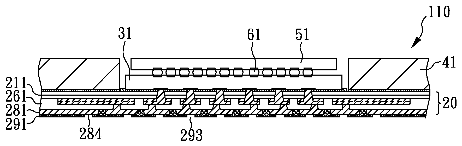
Image

Examples
embodiment 1
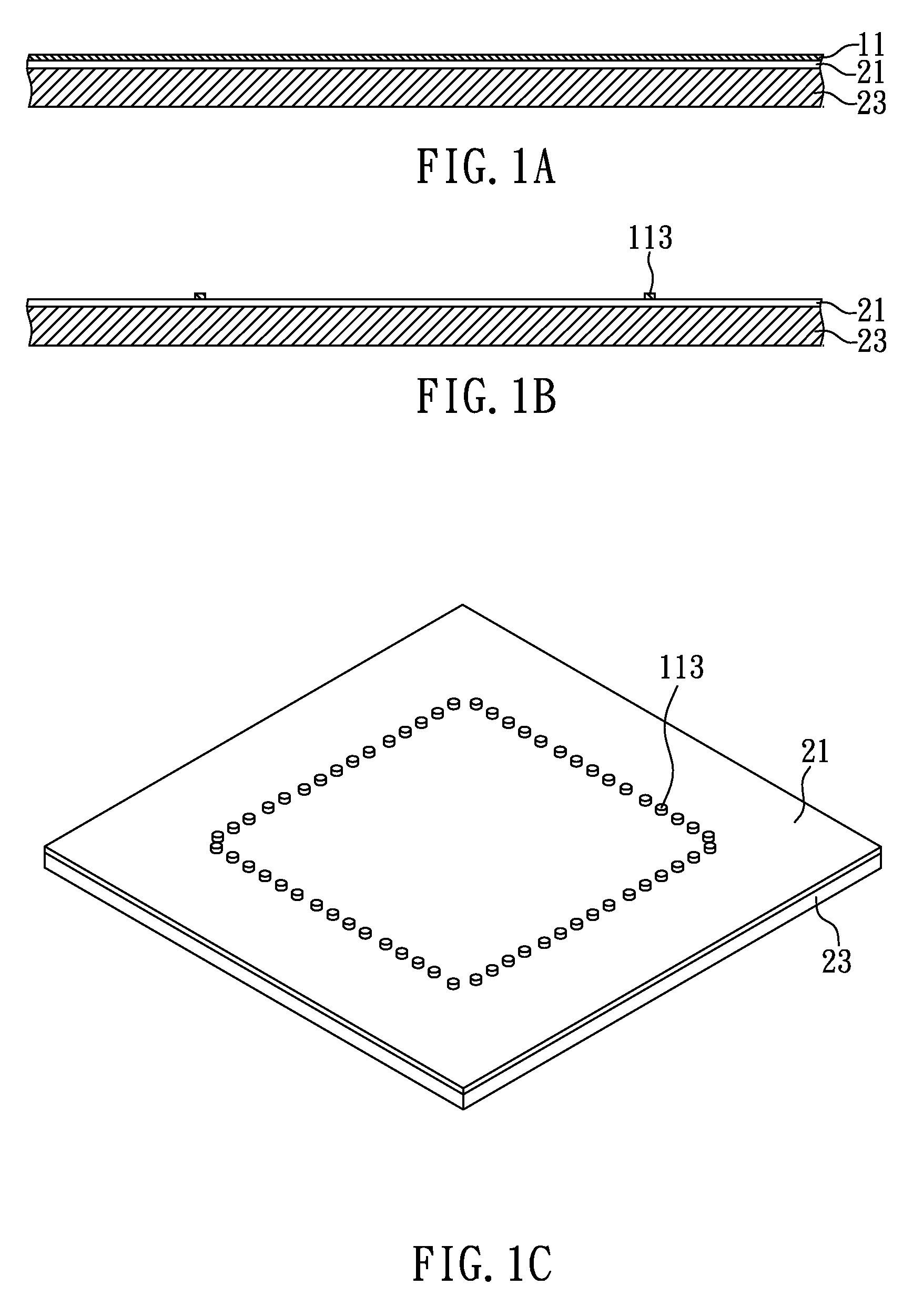
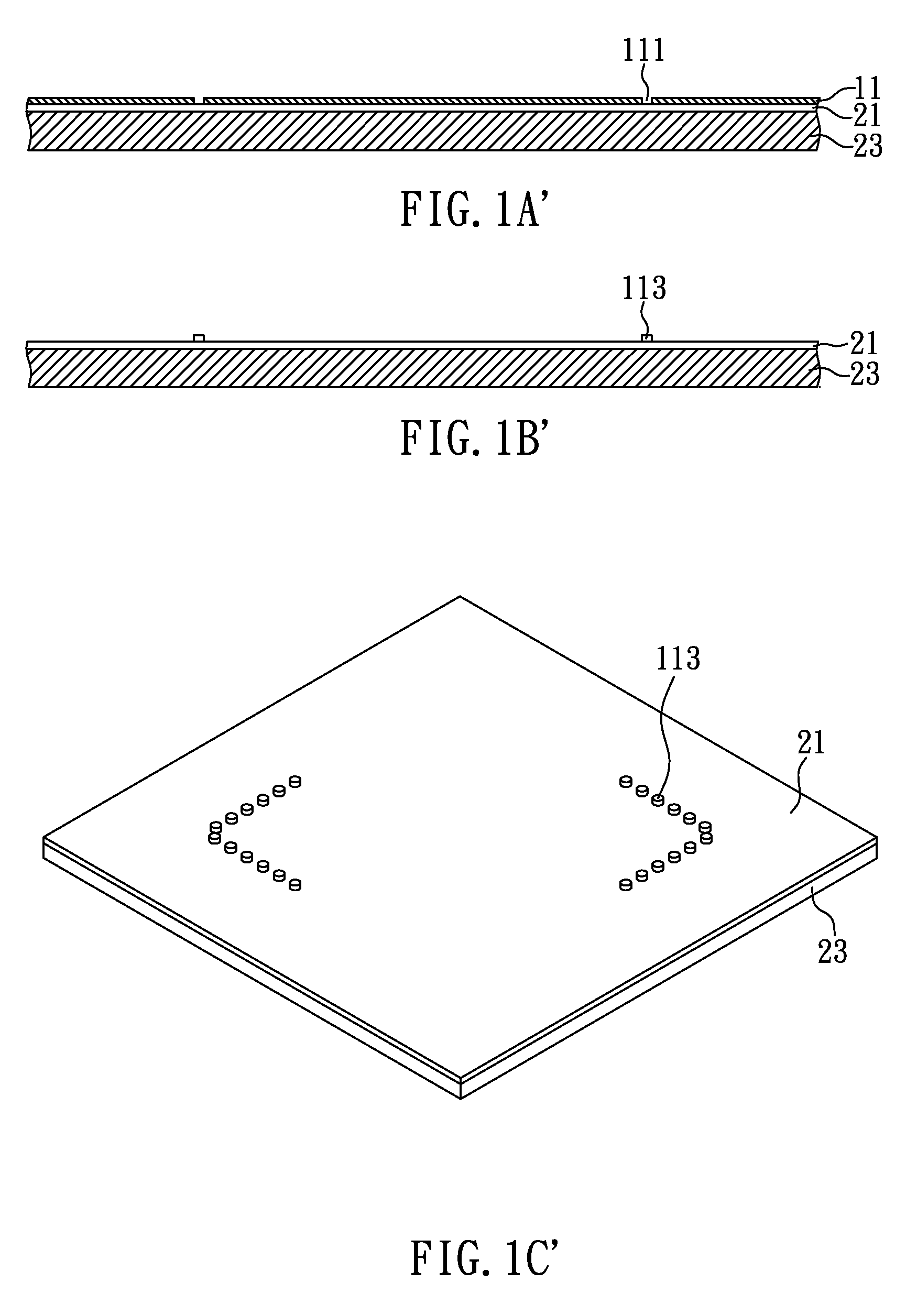
[0036]FIGS. 1A and 1B are cross-sectional views showing a method of forming a stopper on a dielectric layer in accordance with an embodiment of the present invention, and FIG. 1C is a top view corresponding to FIG. 1B.
[0037]FIG. 1A is a cross-sectional view of a laminate that includes metal layer 11, dielectric layer 21 and support plate 23. Metal layer 11 is illustrated as a copper layer with a thickness of 50 microns. However, metal layer 11 can also be made of other various metal materials and is not limited to a copper layer. Besides, metal layer 11 can be deposited on dielectric layer 21 by numerous techniques including lamination, electroplating, electroless plating, evaporating, sputtering, and their combinations as a single layer or multiple layers, and preferably has a thickness in a range of 10 to 200 microns.
[0038]Dielectric layer 21 typically is made of epoxy resin, glass-epoxy, polyimide and the like and has a thickness of 50 microns. In this embodiment, dielectric laye...
embodiment 2
[0063]FIGS. 6A-6D are cross-sectional views showing a method of making a hybrid wiring board with an electrical connection between the first conductive traces and the stiffener in accordance with another embodiment of the present invention.
[0064]For purposes of brevity, any description in Embodiment 1 is incorporated herein insofar as the same is applicable, and the same description need not be repeated.
[0065]FIG. 6A is a cross-sectional view of the structure which is manufactured by the steps shown in FIGS. 1A-3A.
[0066]FIG. 6B is a cross-sectional view of the structure in which support plate 23 is thinned to form metal layer 24 with a desired thickness. Metal layer 24 is illustrated as a copper layer with a thickness of about 15 microns, and dielectric layer 21 is considered first dielectric layer 211 of build-up circuitry.
[0067]FIG. 6C is a cross-sectional view of the structure showing first via openings 213 formed through first dielectric layer 211 and adhesive 131. First via ope...
embodiment 3
[0071]FIGS. 7A and 7B are cross-sectional and top views, respectively, of hybrid wiring board 103 with placement guide 115 in close proximity to the outer peripheral edges of stiffener 41 in accordance with yet another embodiment of the present invention.
[0072]In this embodiment, hybrid wiring board 103 is manufactured in a manner similar to that illustrated in Embodiment 1, except that placement guide 115 is simultaneously formed during stopper 113 formation by removing selected portions of metal layer 11 to accurately confine the placement location of stiffener 41. Placement guide 115 extends from first dielectric layer 211 beyond the attached surface of stiffener 41 in the upward direction and is laterally aligned with and laterally extends beyond four outer lateral surfaces of stiffener 41 in the lateral directions. Placement guide 115 is illustrated as plural metal posts and conforms to four outer sides of stiffener 41 in lateral directions. However, placement guide 115 is not ...
PUM
| Property | Measurement | Unit |
|---|---|---|
| height | aaaaa | aaaaa |
| thickness | aaaaa | aaaaa |
| thickness | aaaaa | aaaaa |
Abstract
Description
Claims
Application Information
 - R&D
- Intellectual Property
- Life Sciences
- Materials
- Tech Scout
- Unparalleled Data Quality
- Higher Quality Content
- 60% Fewer Hallucinations
Browse by: Latest US Patents, China's latest patents, Technical Efficacy Thesaurus, Application Domain, Technology Topic, Popular Technical Reports.
© 2025 PatSnap. All rights reserved.Legal|Privacy policy|Modern Slavery Act Transparency Statement|Sitemap|About US| Contact US: help@patsnap.com