Mask blank, transfer mask, method of manufacturing a transfer mask, and method of manufacturing a semiconductor device
- Summary
- Abstract
- Description
- Claims
- Application Information
AI Technical Summary
Benefits of technology
Problems solved by technology
Method used
Image

Examples
example
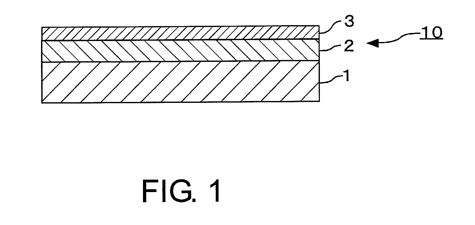
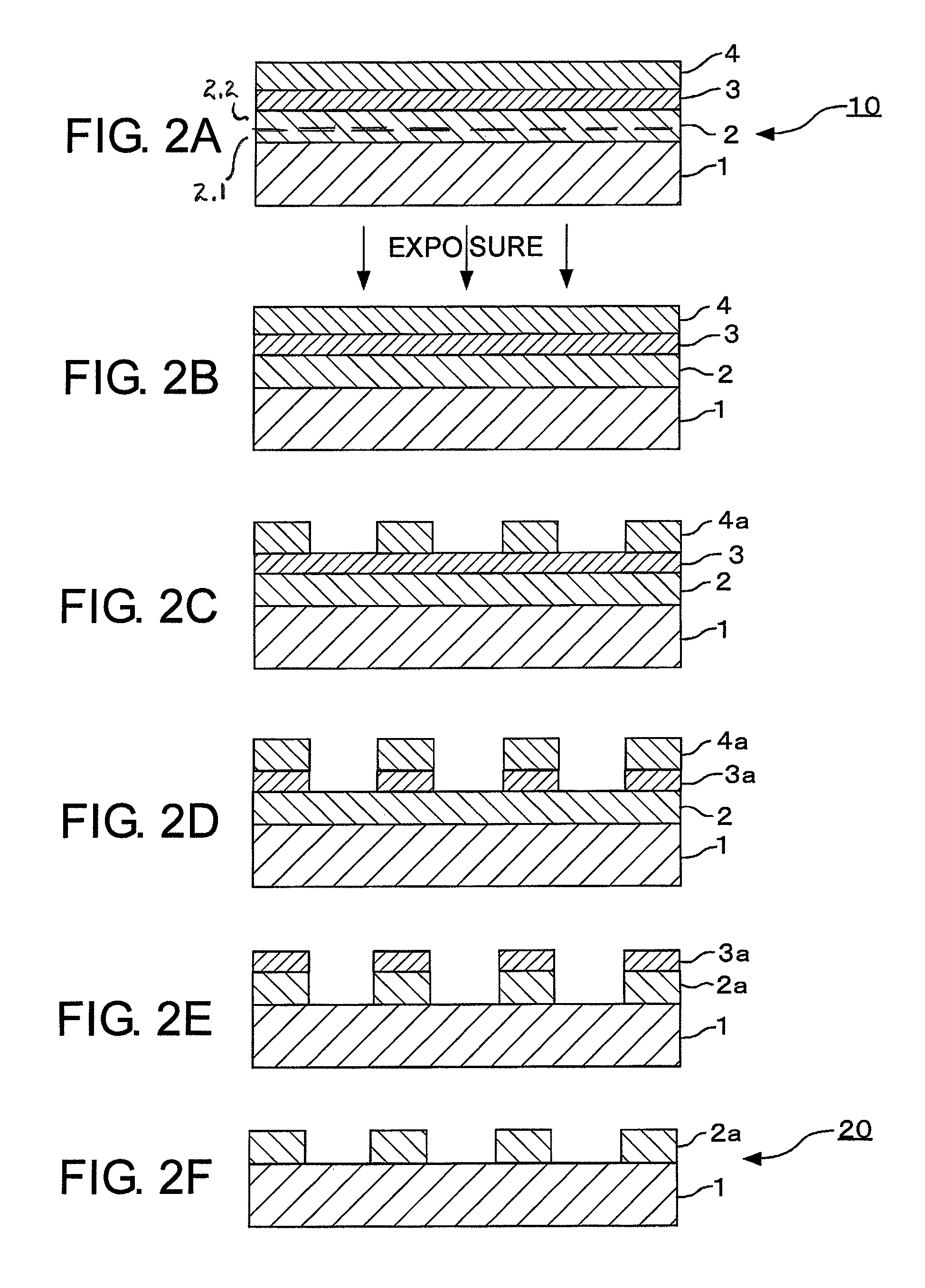
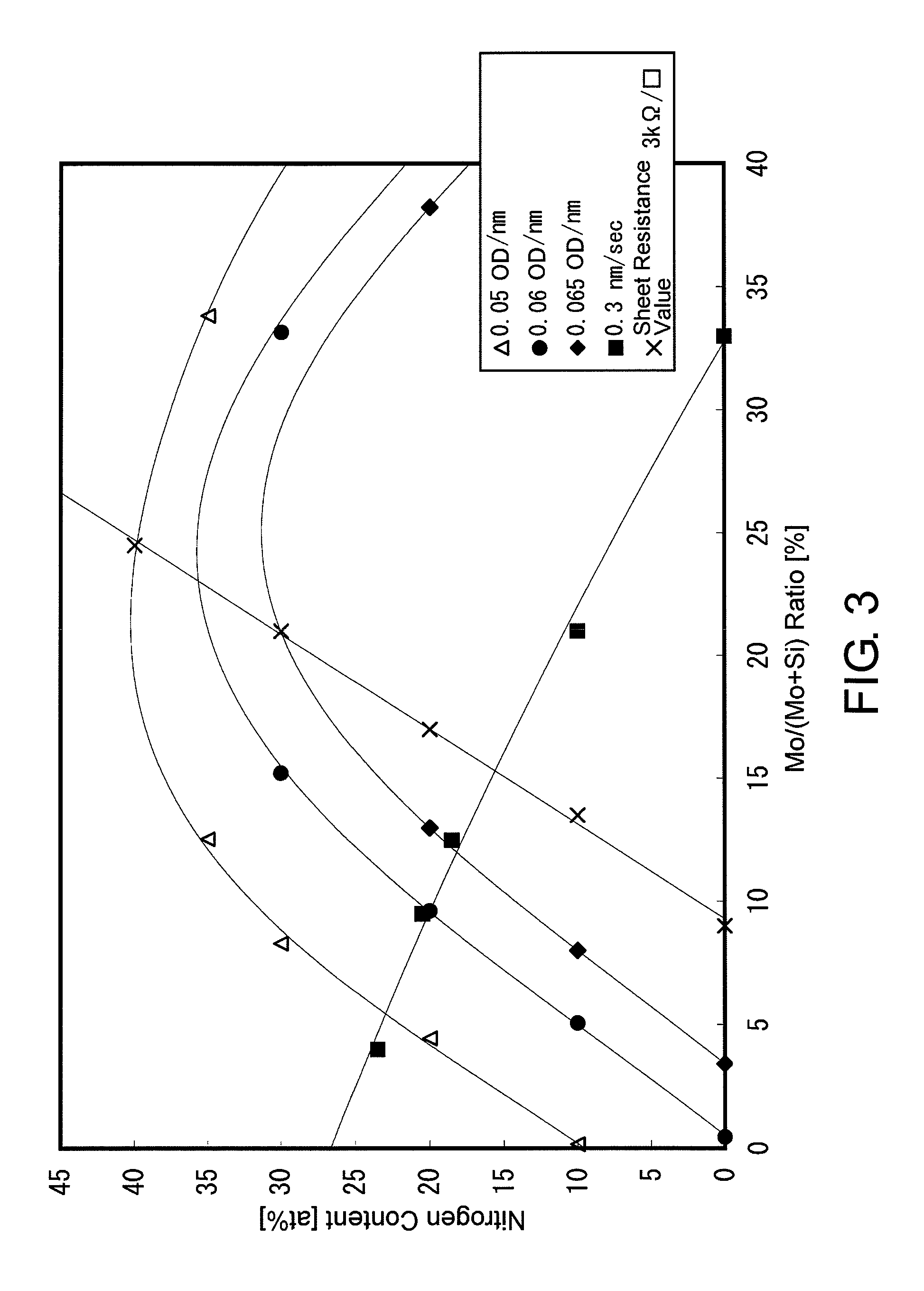
[0109]In a single-wafer sputtering apparatus, using a mixed target of molybdenum (Mo) and silicon (Si) (at % ratio Mo:Si=13:87 ) as a sputtering target, reactive sputtering (DC sputtering) was carried out in a mixed gas atmosphere of argon and nitrogen, thereby forming a MoSiN film (lower layer (light-shielding layer)) to a thickness of 47 nm on a transparent substrate 1 made of synthetic quartz glass. Then, using a Mo / Si target (at % ratio Mo:Si=13:87), reactive sputtering (DC sputtering) was carried out in a mixed gas atmosphere of argon and nitrogen, thereby forming a MoSiN film (upper layer (front-surface antireflection layer)) to a thickness of 13 nm on the lower MoSiN film. In this manner, there was formed a light-shielding film 2 (total thickness: 60 nm) for ArF excimer laser light (wavelength: 193 nm) having a laminated structure. As illustrated only in FIG. 2A, but as applicable to the structure of the light shielding film in FIGS. 2B-2E, the laminated layer comprises a low...
PUM
| Property | Measurement | Unit |
|---|---|---|
| wavelength | aaaaa | aaaaa |
| wavelength | aaaaa | aaaaa |
| OD | aaaaa | aaaaa |
Abstract
Description
Claims
Application Information
 - R&D
- Intellectual Property
- Life Sciences
- Materials
- Tech Scout
- Unparalleled Data Quality
- Higher Quality Content
- 60% Fewer Hallucinations
Browse by: Latest US Patents, China's latest patents, Technical Efficacy Thesaurus, Application Domain, Technology Topic, Popular Technical Reports.
© 2025 PatSnap. All rights reserved.Legal|Privacy policy|Modern Slavery Act Transparency Statement|Sitemap|About US| Contact US: help@patsnap.com