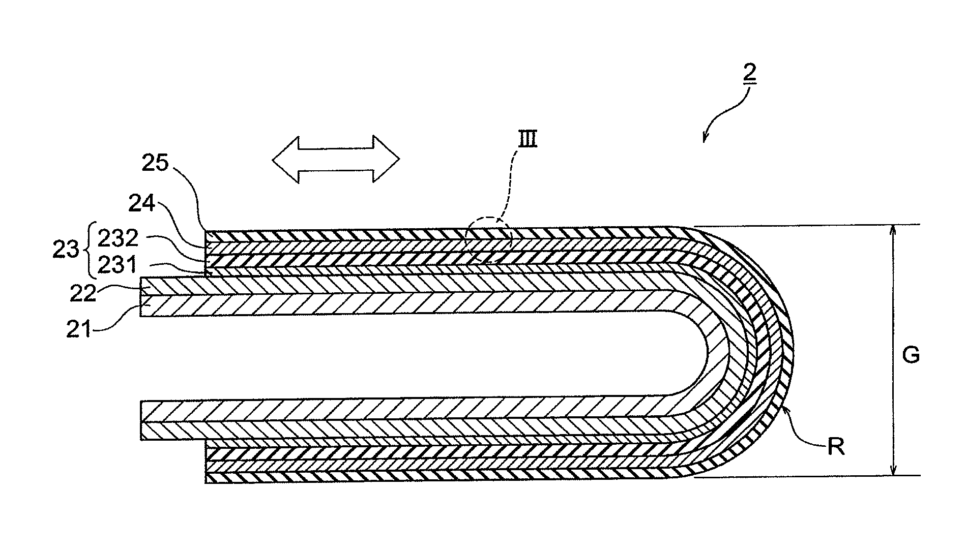
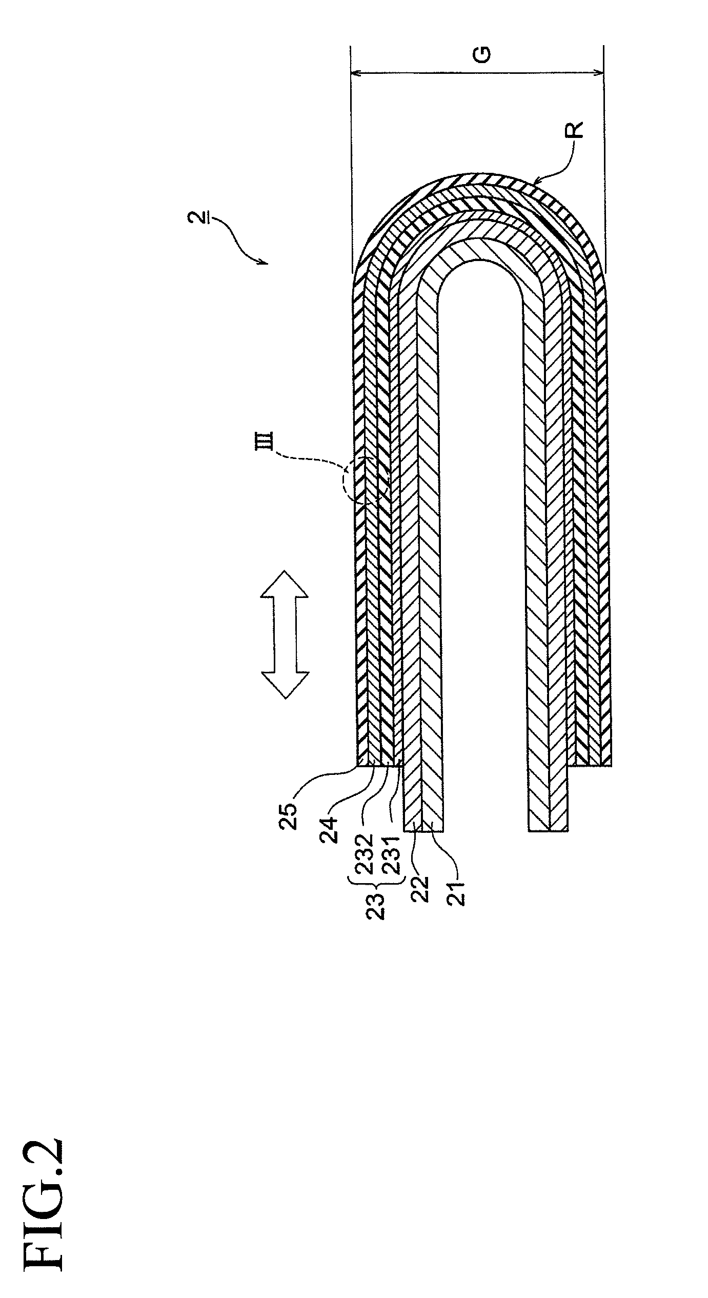
Flexible printed board and method of manufacturing same
a printing board and flexible technology, applied in the direction of printed circuit manufacturing, printed circuit aspects, cross-talk/noise/interference reduction, etc., can solve the problems of insufficient improvement of affecting the bendability of flexible printed circuit boards, and not being considered above-described flexible printed circuit boards, so as to achieve stress concentration, the effect of improving the bendability of flexible printed boards
- Summary
- Abstract
- Description
- Claims
- Application Information
AI Technical Summary
Benefits of technology
Problems solved by technology
Method used
Image

Examples
example 1
[0072]In terms of Example 1, ten samples of flexible printed boards each having the same configuration as the above embodiments were prepared (Samples 1 to 10).
[0073]For these samples according to Example 1, the insulating substrates were composed of polyimide, the circuit wirings were composed of copper, the circuit protection layers were composed of coverlay films, the shield conductive layers were composed of silver paste, and the shield insulating layers were composed of insulating ink. Note that the adhesion layers of the coverlay films were composed of adhesive of epoxy-base resin, and the insulating films were composed of polyimide. Also note that, as the binder of the silver paste, polyester-base resin having viscosity of approximately 200 [dPa·s at 25° C.] to 300 [dPa·s at 25° C.] was used. Still also note that, as the insulating ink, polyester-base resin having viscosity of approximately 50 [dPa·s at 25° C.] to 150 [dPa·s at 25° C.] was used.
[0074]The thicknesses were set ...
examples 2 to 5
[0089]For Examples 2 to 5, as shown in Table 1, each ten samples having the same configuration as Example 1 were prepared with the exception of the tensile elastic modulus E2 of the shield insulating layer being 1.9 [GPa], 2.4 [GPa], 2.88 [GPa], and 3.1 [GPa], respectively.
[0090]Slide test was performed for each sample according to these Examples 2 to 5 in the similar manner as Example 1. Results for Examples 2 to 5 are shown in Table 1 and FIG. 9.
example 6
[0091]For Example 6, each ten samples having the same configuration as Example 1 were prepared with the exception of the thickness of the adhesion layer of the coverlay film being 30 [μm] (Samples 1 to 10). Slide test was performed for each sample according to these samples of Example 6 in the similar manner as Example 1. Results for Example 6 are shown in Table 2 and FIG. 10. Note that the graph of FIG. 10 is plotted with each cycle number at the time of wire breaking for Samples 1 to 10 of Example 6 (likewise also in Examples 7 to 10 and Comparative Examples 3 and 4).
[0092]
TABLE 2Comparative ComparativeExample 6Example 7Example 8Example 9Example 10Example 3Example 4Tensile elastic modulus2.42.42.42.42.42.42.4E1 [GPa] of shieldconductive layerTensile elastic modulus1.81.92.42.883.11.53.5E2 [GPa] of shieldinsulating layerE2 / E10.750.791.001.201.290.631.46CycleSample 1 364981400000400000400000339879197308193475number atSample 2 353486373329400000340410339007172681178999the time ofSamp...
PUM
 Abstract
Description
Claims
Application Information
 - R&D
- Intellectual Property
- Life Sciences
- Materials
- Tech Scout
- Unparalleled Data Quality
- Higher Quality Content
- 60% Fewer Hallucinations
Browse by: Latest US Patents, China's latest patents, Technical Efficacy Thesaurus, Application Domain, Technology Topic, Popular Technical Reports.
© 2025 PatSnap. All rights reserved.Legal|Privacy policy|Modern Slavery Act Transparency Statement|Sitemap|About US| Contact US: help@patsnap.com