Solid-state image capturing device, method for manufacturing the same and electronic information device
a solid-state image and capture device technology, applied in the direction of radio frequency controlled devices, instruments, television systems, etc., can solve the problems of not only deteriorating the luminance shading characteristic, but also different luminance shading characteristics in each pixel, so as to improve the light receiving sensitivity and luminance shading characteristic, improve the uniformity and improve the effect of luminance shading characteristi
- Summary
- Abstract
- Description
- Claims
- Application Information
AI Technical Summary
Benefits of technology
Problems solved by technology
Method used
Image
Examples
embodiment 1
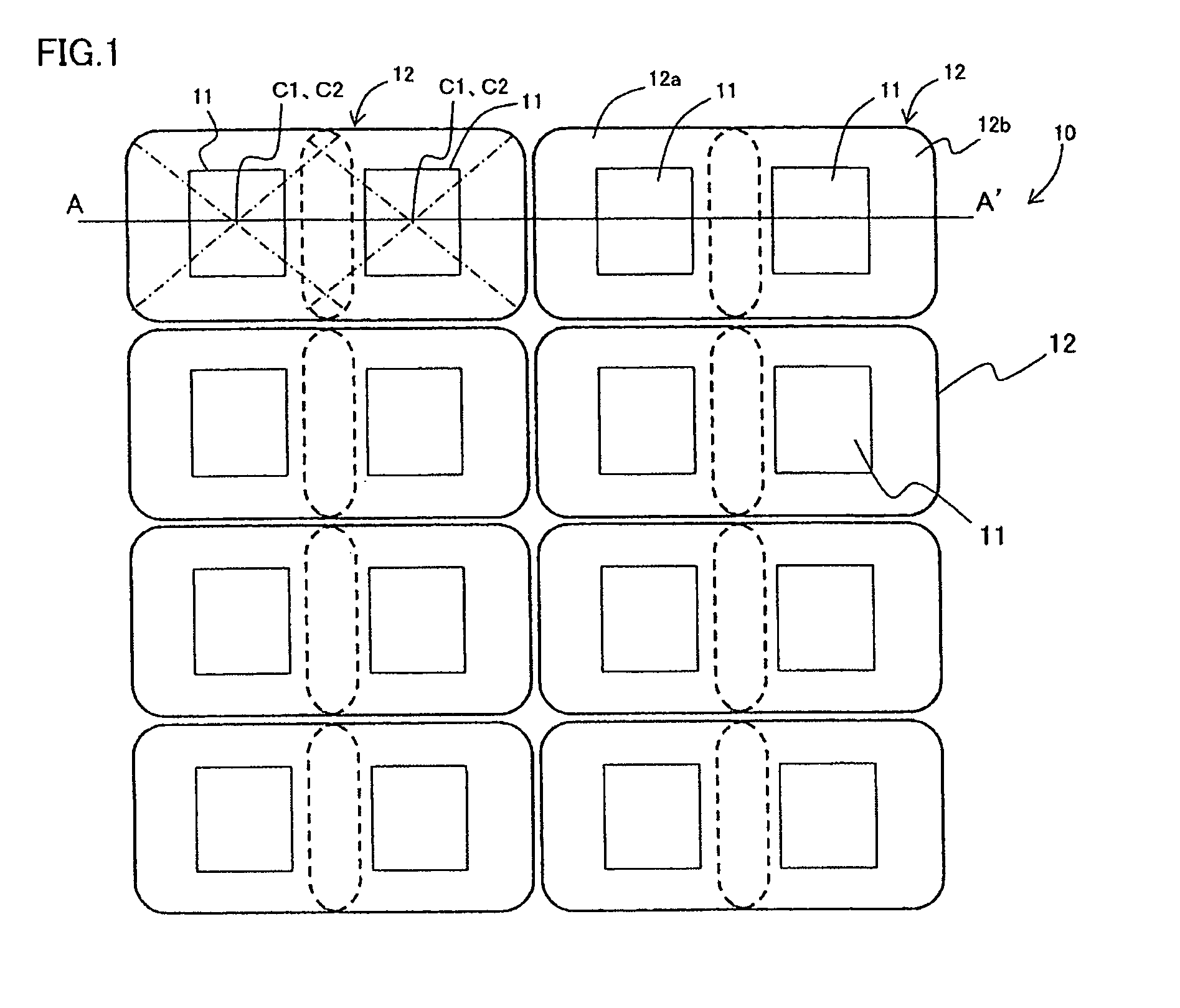
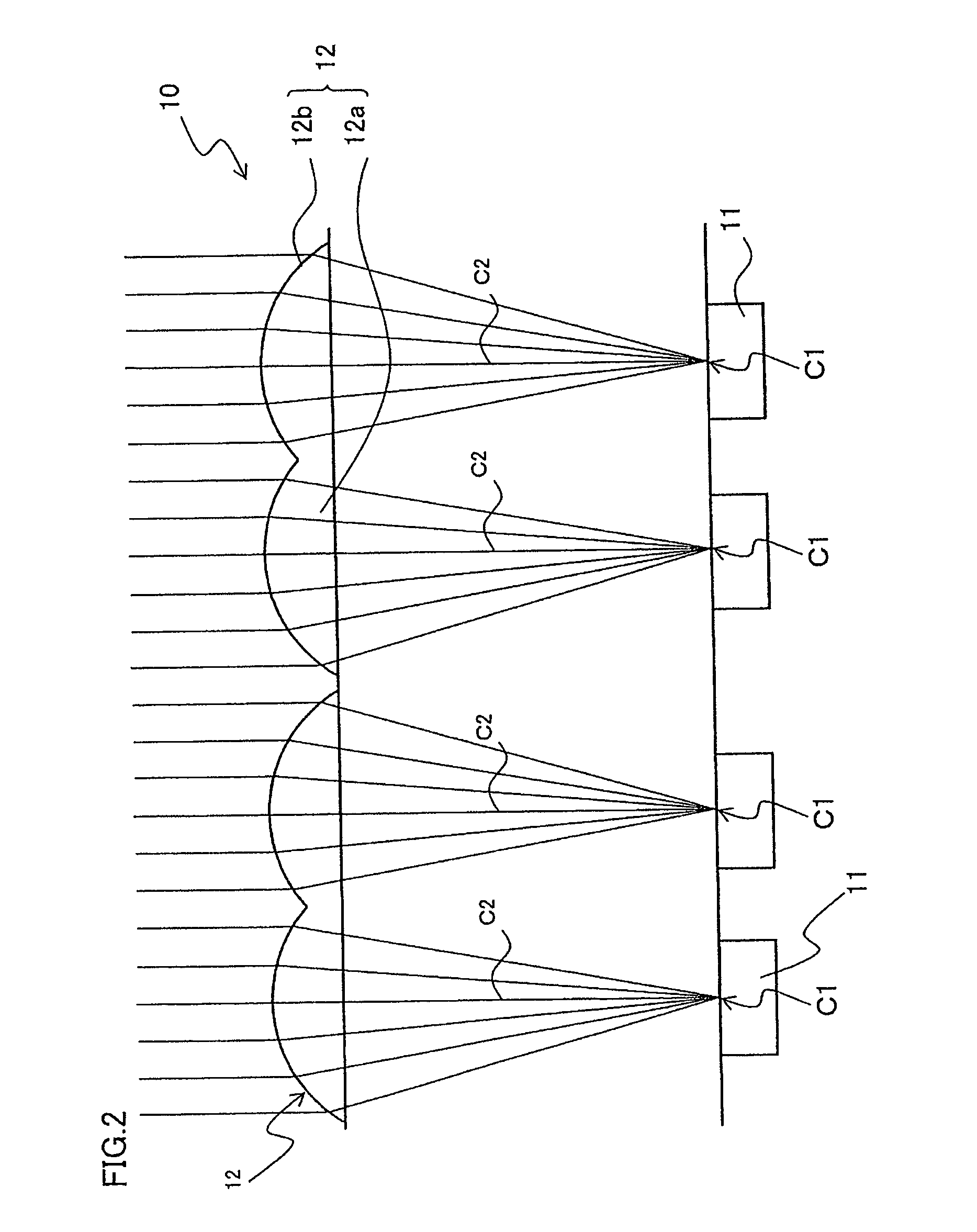
[0085]FIG. 1 is a plane view showing an exemplary essential structure of a pixel section in a solid-state image capturing device 10 according to Embodiment 1 of the present invention. FIG. 2 is a longitudinal cross-sectional view schematically showing a portion cut at line A-A′ in FIG. 1.
[0086]In FIG. 1 and FIG. 2, the solid-state image capturing device 10 according to Embodiment 1 includes: a plurality of photodiodes 11 as a plurality of light receiving sections arranged such that the locations thereof in each pixel unit are different according to a sequence; and microlens 12 arranged above the plurality of photodiodes 11 so as to correspond to the plurality of photodiodes 11. When some or all of the adjacent microlenses 12 among the microlenses 12 are close to each other such that the peripheral portions of the microlenses 12 overlap, the microlenses 12 having a shape of lens with the overlapped lens portions thereof straightly cut off are formed so the microlens 12 are adjacent t...
embodiment 2
[0100]Embodiment 2 will describe a case in which the first microlens 2a and the second microlens 2b according to Embodiment 1 are circular (or approximate circular or elliptical) in a plane view, and the curvature thereof is constant.
[0101]FIG. 5 is a plane view showing an exemplary essential structure of a pixel section in a solid-state image capturing device 20 according to Embodiment 2 of the present invention. FIG. 6 is a longitudinal cross-sectional view schematically showing a portion cut at line B-B′ in FIG. 5.
[0102]In the solid-state image capturing device 20 according to Embodiment 2 in FIG. 5 and FIG. 6, microlenses 22 are arranged above photodiodes 21 making up pixels so as to correspond to the photodiodes 21. The locations of the photodiodes 21 are different according to a sequence in each pixel unit. In a plane view, the center position C1 of a photodiode 21 matches the optical axis C2 of a corresponding microlens 22. The curvature of a microlens 22 in the solid-state i...
embodiment 3
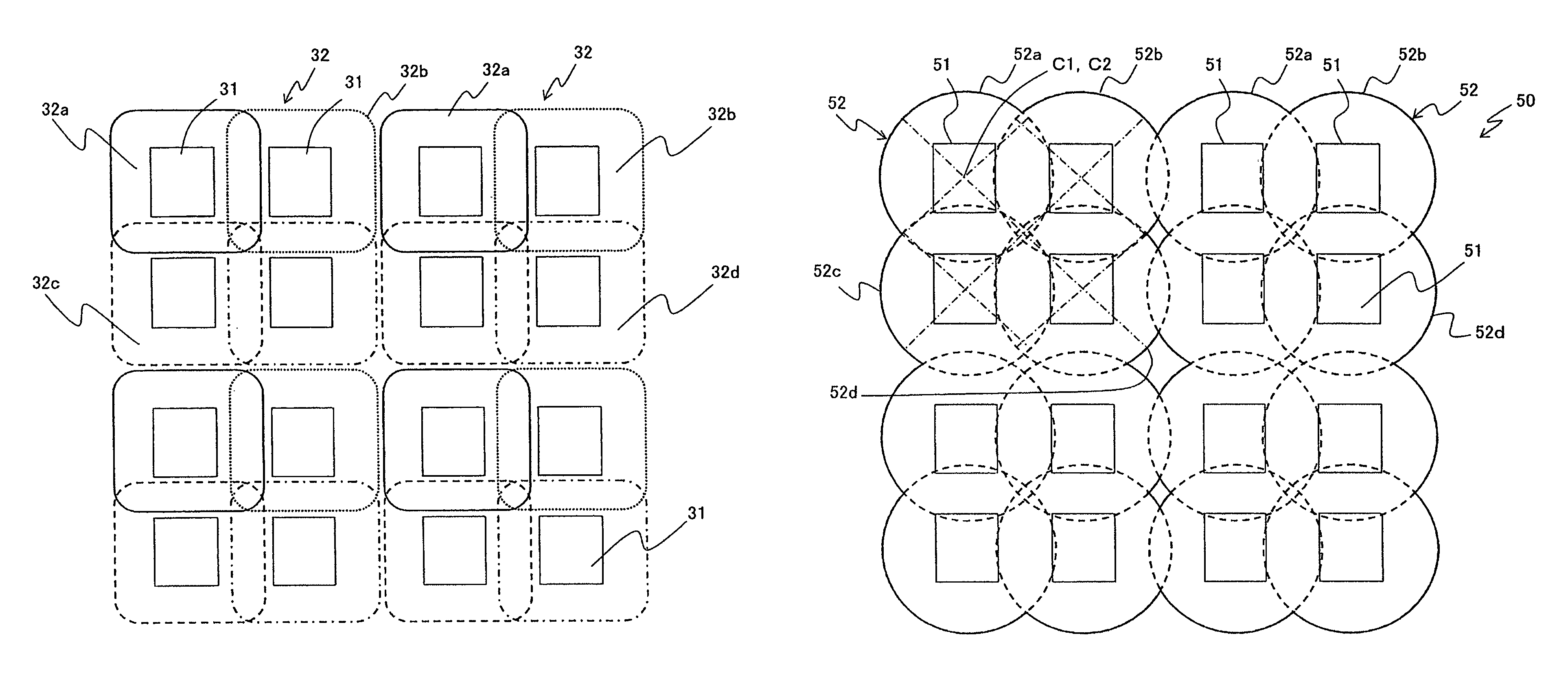
[0116]Embodiments 1 and 2 have described the case in which photodiodes 11 or 21 are grouped in two pixels, and the locations of the photodiodes 11 or 21 in each two-pixel unit are different according to a sequence only in a row direction (horizontal direction). Embodiment 3 will describe a case in which photodiodes are grouped in four pixels, and the locations of the photodiodes in each four-pixel unit are different according to a sequence in both a row direction (horizontal direction) and a column direction (vertical direction).
[0117]FIG. 8 is a plane view showing an exemplary essential structure of a pixel section in a solid-state image capturing device 30 according to Embodiment 3 of the present invention.
[0118]In the solid-state image capturing device 30 according to Embodiment 3 in FIG. 8, one microlens 32 is provided above four photodiodes 31 making up four pixels in a lateral direction and a longitudinal direction so as to correspond to the four photodiodes 31. This one micro...
PUM
 Abstract
Description
Claims
Application Information
 - R&D
- Intellectual Property
- Life Sciences
- Materials
- Tech Scout
- Unparalleled Data Quality
- Higher Quality Content
- 60% Fewer Hallucinations
Browse by: Latest US Patents, China's latest patents, Technical Efficacy Thesaurus, Application Domain, Technology Topic, Popular Technical Reports.
© 2025 PatSnap. All rights reserved.Legal|Privacy policy|Modern Slavery Act Transparency Statement|Sitemap|About US| Contact US: help@patsnap.com


