
Method and apparatus for testing 3D integrated circuits

a technology of integrated circuits and methods, applied in the field of scan-based design and testing, can solve the problems of increasing test cost, i/o pads not available to all dies (layers), and test data volume and test application time (that affect test cost) have increased dramatically, so as to reduce test cost and high data rate

Inactive Publication Date: 2013-08-27
SYNTEST TECH
View PDF7 Cites 34 Cited by
  • Summary
  • Abstract
  • Description
  • Claims
  • Application Information

AI Technical Summary

Benefits of technology

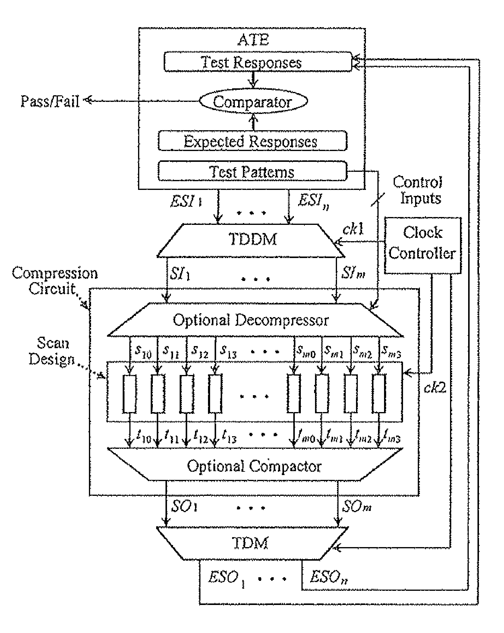
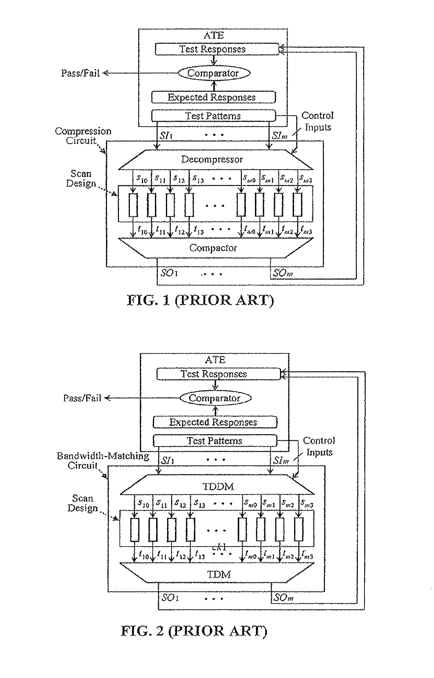
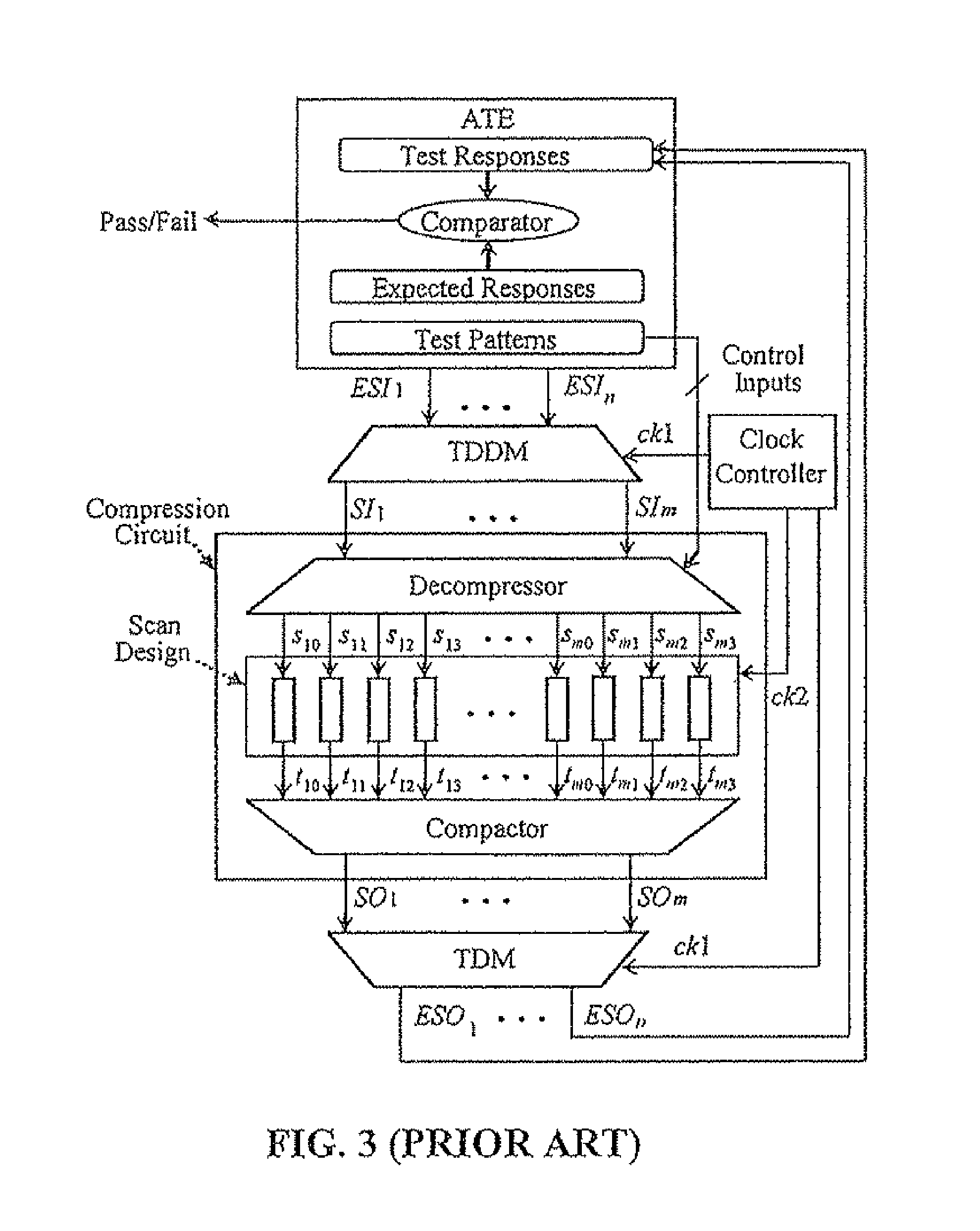
The present invention describes a method to apply the bandwidth-matching or time-division demultiplexing / multiplexing (TDDM / TDM) technique to 3DIC testing. This technique helps reduce test cost by adhering to the strict pad count limit allocated to a 3D chip during both pre-bond and post-bond testing. It takes advantage of the high-speed external scan input / output ports (I / O pads) in a scan-based integrated circuit, which are designed to operate at very high frequencies, while the scan chains usually only operate at a much lower frequency. The method allows for the same number of test cycles and I / O pad count as if the entire chip contains only one die during post-bond testing. It also reduces the number of through-silicon vias (TSVs) and the same test patterns can be reused during pre-bond and post-bond testing. The method further reduces overall 3D test cost by applying test data for pre-bond testing on high-speed I / O pads and using bandwidth that would otherwise be left from a die when finishing testing a die containing two or more modules.

Problems solved by technology

In a typical 3D chip, I / O pads are not available to all dies (layers).
Due to increased SOC complexity and gate count, test data volume and test application time (that affect test cost) have increased dramatically even for single stuck-at faults.
Such requirement further drives up test cost.
Since one single 3D chip can contain two or more dies, 3DIC designers are now facing an unprecedented challenge of managing both test cost and I / O pad count limit during pre-bond and post-bond testing.
Test cost is dictated by test application time and test data volume, whereas I / O pads are limited not only by the available number of pads presents on the bottom die but also by the need to route those bottom pads via TSVs to provide access to signals on other (upper) dies.
This approach increases test cost drastically.
This approach when combined with scan compression, unfortunately, may cause fault coverage loss as aliasing may occur more often in the SOC design.
This may pose a serious problem as a 2n test cost is economically infeasible.
How to fully utilize scan technology in a 3DIC yet still to reduce test cost and improve fault coverage is now becoming a very important challenge.

Method used


Image

  • Method and apparatus for testing 3D integrated circuits
  • Method and apparatus for testing 3D integrated circuits
  • Method and apparatus for testing 3D integrated circuits

Examples


first embodiment

[0057]FIG. 7 shows a circuit diagram of the present invention for testing a 3DIC with 2 dies and 10 modules each. The first architecture includes a TDDM circuit 701 and a TDM circuit 702, both running at 20 MHz. In the architecture, a 1-to-1 dedicated bus 703 that transports test data in and out of a module on each die is not shared with other modules. The TDDM circuit couples a 1-bit register (flip-flop) to each module scan input, so a test pattern applied on the external scan input port can be latched in the register within the module. The TDM circuit includes a multiplexer which is coupled to all module scan chain outputs so the captured test response from one die can be shifted out to ATE for analysis one at a time.

second embodiment

[0058]FIG. 8 shows a circuit diagram of the present invention for testing a 3DIC. The second 3DIC test architecture includes a TDDM circuit 801 and a TDM circuit 802, both running at 200 MHz. Unlike Architecture 1, this architecture uses a 1-to-10 (or a 10-to-1) dedicated bus to transport test data in (or out of) a module on each die. This requires that each TDDM / TDM circuit is a high-speed 10-bit deserializer / serializer that operates at 200 MHz. With this architecture, the single scan chain can now be split into 10 balanced short scan channels, resulting in a 10× reduction in test application time.

third embodiment

[0059]FIG. 9 shows a circuit diagram of the present invention for testing a 3DIC. The third 3DIC test architecture includes a TDDM circuit 901 and a TDM circuit 902, both running at 200 MHz. Unlike Architectures 1 and 2, this architecture uses a 10-to-10 shared bus that transports test data in and out of all modules on each die in parallel. The TDDM circuit now couples a 10-bit register to the shared bus, so a 10-bit test pattern, instead of 1-bit as in Architecture 1, applied on the external scan input port can be latched in the register within the module one at a time. The TDM circuit includes a multiplexer which is coupled to all module scan chain outputs so the captured test response from one die can be shifted out to ATE for analysis one at a time. This will require operating the bus at 200 MHz to shift test data in and out of each module. With this architecture, the single scan chain can now also be split into 10 balanced short scan channels, resulting in a reduction of 10× in...


PUM


Abstract

A method and apparatus for testing a scan-based 3D integrated circuit (3DIC) using time-division demultiplexing / multiplexing allowing for high-data-rate scan patterns applied at input / output pads converting into low-data-rate scan patterns applied to each embeddded module in the 3DIC. A set of 3D design guidelines is proposed to reduce the number of test times and the number of through-silicon vias (TSVs) required for both pre-bond testing and post-bond testing. The technique allows reuse of scan patterns developed for pre-bond testing of each die (layer) for post-bond testing of the whole 3DIC. It further reduces test application time without concerns for I / O pad count limit and risks for fault coverage loss.

Description

FIELD OF THE INVENTION[0001]The present invention generally relates to the field of scan-based design and test using design-for-test (DFT) techniques. Specifically, the present invention relates to the field of scan testing and test compression.BACKGROUND[0002]Three-dimensional (3D) packaging is short for 3D die stacking using through-silicon vias (TSVs), conceptually similar to nails, as opposed to wire-bonds for connecting the dies to the package substrate. A 3D integrated circuit (3DIC) may contain two or more dies (layers), each of which could include a partial or full system-on-chip (SOC) logic that may contain tens to hundreds of millions of gates.[0003]In a typical 3D chip, I / O pads are not available to all dies (layers). Instead, they are only bonded to the bottom layer, and functional signal values must be elevated from the bottom layer to upper layers via TSVs (also referred to as functional TSVs).[0004]Due to increased SOC complexity and gate count, test data volume and t...

Claims


Application Information

Patent Timeline
Patent Type & Authority Patents(United States)
IPC IPC(8): G01R31/28
CPCG01R31/318558G01R31/318572
Inventor WANG, LAUNG-TERNGTOUBA, NUR A.HSIAO, MICHAEL S.JIANG, ZHIGANGWU, SHIANLING
Owner SYNTEST TECH
Learn More