
Gold wire for semiconductor element connection

a technology of semiconductor elements and gold wires, applied in the direction of semiconductor devices, solid-state devices, basic electric elements, etc., can solve the problems of insufficient mechanical strength, difficult maintenance of a loop thereof, and broken bonding wires, so as to improve the workability of semiconductor device manufacturing and product yield, the effect of reducing the number of defects

Active Publication Date: 2013-04-09
NIPPON MICROMETAL CO LTD +1
View PDF13 Cites 0 Cited by
  • Summary
  • Abstract
  • Description
  • Claims
  • Application Information

AI Technical Summary

Benefits of technology

The present invention provides a gold wire for semiconductor element connection that solves the problem of poor bondability and mechanical characteristics. The gold wire contains specific amounts of Ca, rare earth elements, Ti, V, Cr, Hf, Nb, W, and Zr to improve strength, roundness, and bondability simultaneously. This results in a bonding wire that meets demands for the downsizing of semiconductor devices and the narrowing of pad electrodes, thereby improving workability and product yield.

Problems solved by technology

Although strength of bonding wires is increased by work hardening at the time of drawing process, sufficient mechanical strength is not obtained with pure gold, and thus trace amounts of different elements are added thereto.
The downsizing of the wire diameter will cause the bonding wire to be broken during the manufacture thereof due to the strength thereof being insufficient at the time of drawing, or will make maintenance of a loop thereof difficult at the time of mounting process, such as wire bonding, resin encapsulation, etc.
Additive elements generally used for the bonding wire, however, are easily oxidized at the time of formation of FABs.
Thus, adding large amounts of the additive elements to the bonding wire will deteriorate the bondability of the first bonding.
Recently, roundness of a press-bonded ball formed by press-bonding a FAB onto a pad has become an issue in connection with the first bonding.
If pad pitches of electrodes on semiconductor chips become narrow with the downsizing of semiconductor chips, then the risk of occurrence of short-circuit caused by the press-bonded balls running over the adjacent edges of pads is increased in the event that shapes of the press-bonded balls in the first bonding get out of round.
Bonding wires containing a high content of Ca or rare earth elements used for those of high strength and high-Young's modulus to meet the downsizing of semiconductor chips have a tendency for the roundness of the resultant press-bonded balls to deteriorate.

Method used


Image

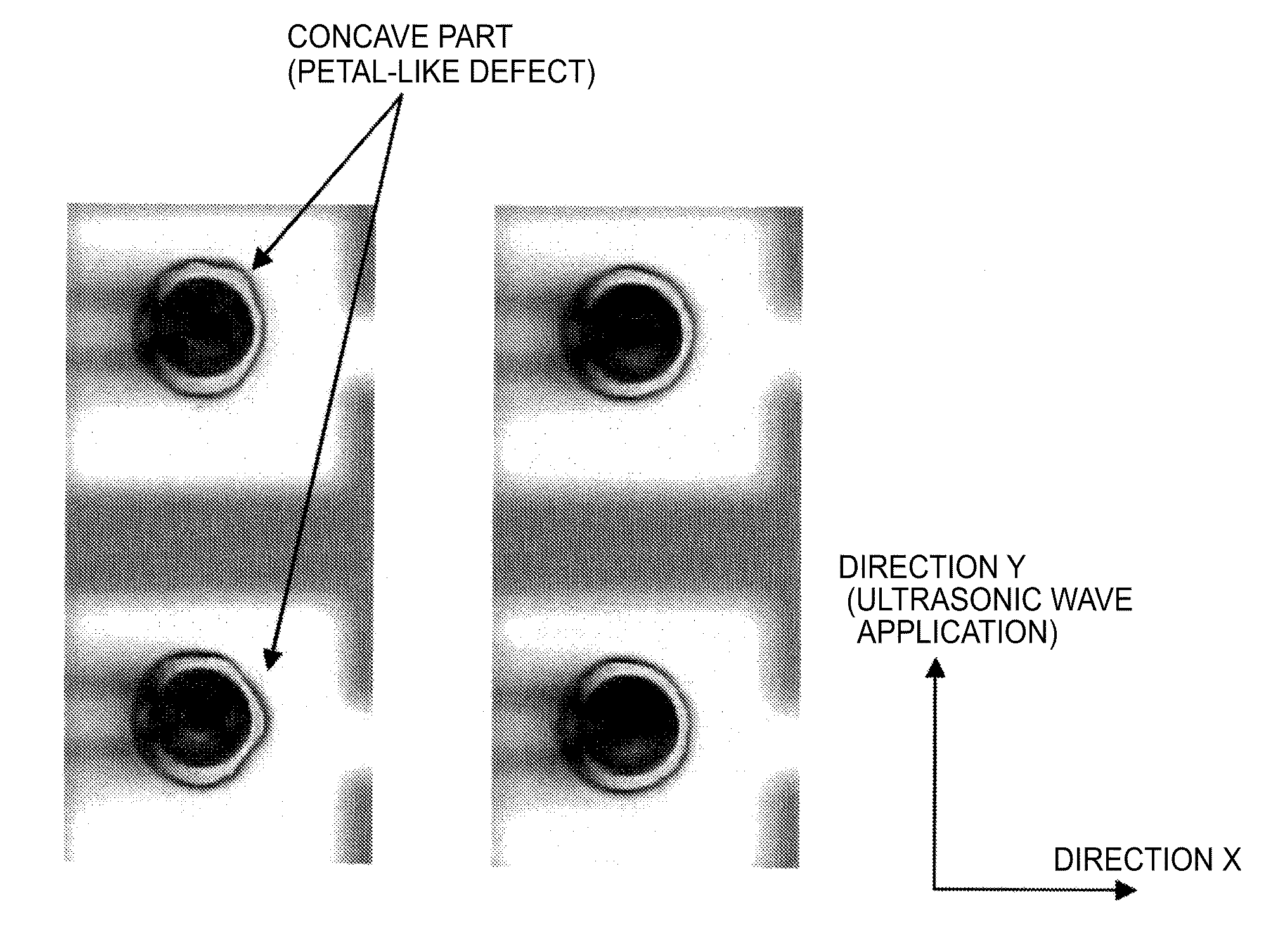
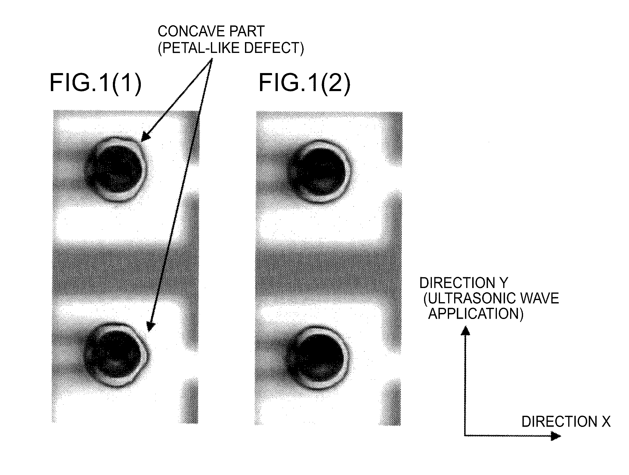
  • Gold wire for semiconductor element connection
  • Gold wire for semiconductor element connection

Examples


examples

[0045]Next is a detailed description of the present invention based on examples, which are only shown by way of example, and the invention is not limited by the examples.

first example

[0046]Samples of bonding wires containing 0.001% by mass of Ca or 0.001% by mass of La were prepared to study the effect of adding Ti and V.

[0047]The above amount of Ca or La was added to a gold material having a purity of 99.9998% or more by mass, and cast into ingots of 5 mm in diameter and 100 mm in length. Likewise, another material was also prepared by adding 0.001% by mass of Ti or V to these elements. After the casting, the composition of each sample was analyzed, and it was confirmed that the Si content was 0.001% or less by mass, and the contents of Ca, rare earth elements, Pb, Sn, Li and Na other than the addition elements were 0.0002% or less by mass.

[0048]Then, the ingots were each rolled to about 2 mm square using a groove rolling device, and drawn to a 0.56 mm in diameter using diamond dies. Subsequently, they were allowed to undergo process annealing at 400° C. for 10 minutes in Ar atmosphere. After that, it was drawn to a 25 μm in diameter at 10 m / min using the diamo...

second example

[0057]For studying the effect of Ca or rare earth elements on the press-bonding shape, the bondability was examined in a fixed range of the Ti content from 0.0015 to 0.004% by mass, depending on the additive amount of Ca or rare earth elements.

[0058]Cast ingots of 6 mm diameter were prepared by adding the predetermined elements to the gold material used in the first example. Then, the ingots were rolled to about 2 mm square using a groove rolling device, and drawn to a 23 μm in diameter using a diamond dies in a lubricating liquid. In the drawing process, a reduction in area per each passage through the die was about 10%, and the work rates of the bonding wires were 99.8%. Thereafter, heat treatment (thermal refining) was continuously performed using a tubular furnace in Ar atmosphere, and then a tensile test of the bonding wires was performed at varying temperatures to adjust the breaking elongation as the breaking elongations were adjusted to 4%

[0059]The bonding test was performed...


PUM

PropertyMeasurementUnit
elastic modulusaaaaaaaaaa
diameteraaaaaaaaaa
Young's modulusaaaaaaaaaa

Abstract

A gold wire for semiconductor element connection having high strength and bondability. The connection has a limited amount of at least one element selected from calcium and rare earth elements, and a limited amount of at least one element selected from a group consisting of titanium, vanadium, chromium, hafnium, niobium, tungsten, and zirconium. The incorporation of a suitable amount of palladium or beryllium is preferred. The incorporation of calcium and rare earth element can improve the strength and young's modulus of a gold wire, and the incorporation of titanium and the like can reduce a deterioration in the roundness of press-bonded shape of press-bonded balls in the first bonding caused by the incorporation of calcium and rare earth elements. The bonding wire can simultaneously realize mechanical properties and bondability capable of meeting a demand for a size reduction in semiconductor and a reduction in electrode pad pitch.

Description

CROSS-REFERENCE TO RELATED APPLICATIONS[0001]This is the U.S. national phase application under 35 U.S.C. §371 of International Patent Application No. PCT / JP2007 / 056011, filed Mar. 23, 2007, and claims the benefit of Japanese Application Nos. 2006-082565, filed Mar. 24, 2006 and 2007-015430 filed Jan. 25, 2007, all of which are incorporated by reference herein. The International Application was published in Japanese on Apr. 10, 2007 as International Publication No. WO 2007 / 111248 A1 under PCT Article 21(2).TECHNICAL FIELD[0002]The present invention relates to a gold wire for semiconductor element connection.BACKGROUND OF THE INVENTION[0003]Bonding wires used as materials for mounting semiconductors, including a gold wire for semiconductor element connection, are materials for connecting a semiconductor chip with external metal terminals. At present, most of such bonding wires are made using a material mainly comprised of gold. The main reason for this is that a so-called “ball bondin...

Claims


Application Information

Patent Timeline
Patent Type & Authority Patents(United States)
IPC IPC(8): H01L23/49
CPCC22C5/02H01L24/45H01L2224/05624H01L2224/45015H01L2224/45144H01L2224/4851H01L2224/85205H01L2224/85206H01L2924/01003H01L2924/01004H01L2924/01006H01L2924/01011H01L2924/01013H01L2924/01014H01L2924/01018H01L2924/0102H01L2924/01022H01L2924/01025H01L2924/01027H01L2924/01028H01L2924/01029H01L2924/01031H01L2924/01038H01L2924/0104H01L2924/01042H01L2924/01046H01L2924/01047H01L2924/01049H01L2924/0105H01L2924/01057H01L2924/01058H01L2924/01059H01L2924/01074H01L2924/01077H01L2924/01078H01L2924/01079H01L2924/01082H01L2924/01105H01L2924/01202H01L2924/01205H01L2924/01327H01L2924/20752H01L2924/01072H01L2924/01024H01L2924/0106H01L2924/01023H01L2924/01041H01L2924/01062H01L2924/00011H01L2924/00014H01L2924/01019H01L2924/01033H01L2924/01044H01L2924/01045H01L2924/01067H01L2924/0107H01L2924/01076H01L2924/00H01L2224/48624H01L2224/48247H01L2224/85439H01L2924/10253H01L2924/013H01L24/43H01L2224/43H01L2224/48639H01L2924/20751H01L2924/00015H01L2924/00013
Inventor KIMURA, KEIICHIUNO, TOMOHIROYAMADA, TAKASHINISHIBAYASHI, KAGEHITO
Owner NIPPON MICROMETAL CO LTD
Learn More