Drive circuit and display device
a drive circuit and display device technology, applied in the field of drive circuits, can solve the problems of affecting the operation of the high voltage side operation amplifier or the low voltage side operation amplifier, and the liquid crystal layer tends to deteriorate, so as to secure the effect of preventing an excessive current from flowing
- Summary
- Abstract
- Description
- Claims
- Application Information
AI Technical Summary
Benefits of technology
Problems solved by technology
Method used
Image

Examples
first embodiment
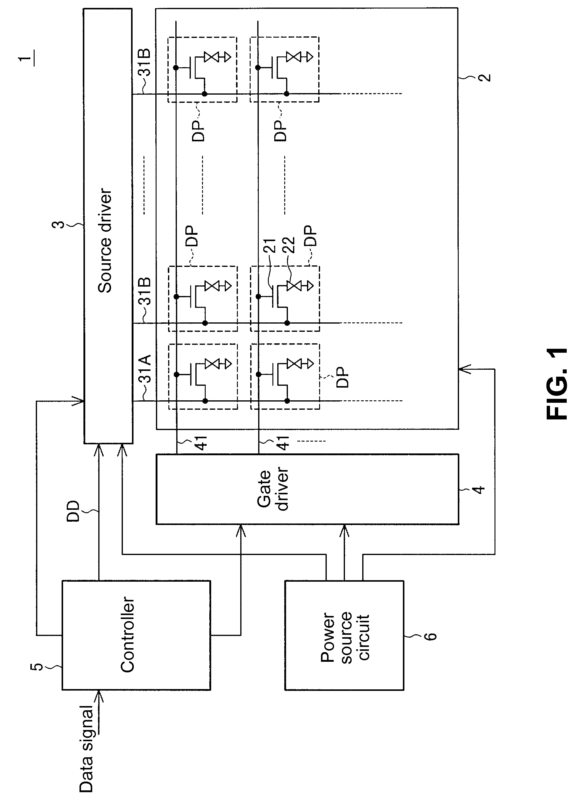
[0039]A first embodiment of the present invention will be explained. FIG. 1 is a block diagram showing a configuration of a liquid crystal display device 1 according to the first embodiment of the present invention.
[0040]As shown in FIG. 1, the liquid crystal display device 1 includes a liquid crystal display panel 2; a source driver 3; a gate driver 4; a controller 5; and a power source circuit 6. The controller 5 or a control unit is provided for controlling operations of the source driver 3 and the gate driver 4.
[0041]In the embodiment, the liquid crystal display panel 2 includes a back light unit (not shown); scanning lines 41 (source lines) arranged in parallel to each other; and data lines 31A and 31B (source lines) arranged to be away from and cross the scanning lines 41.
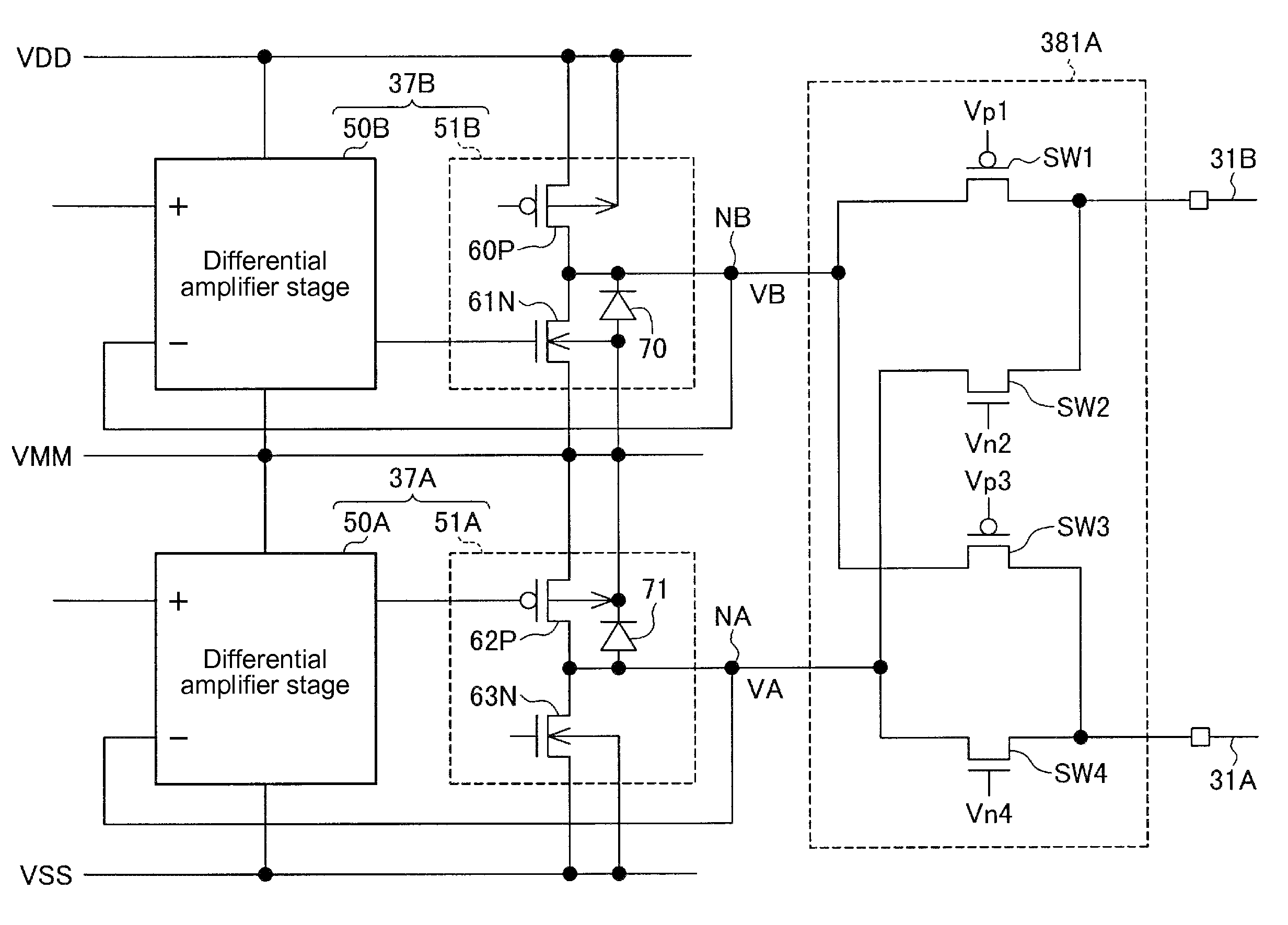
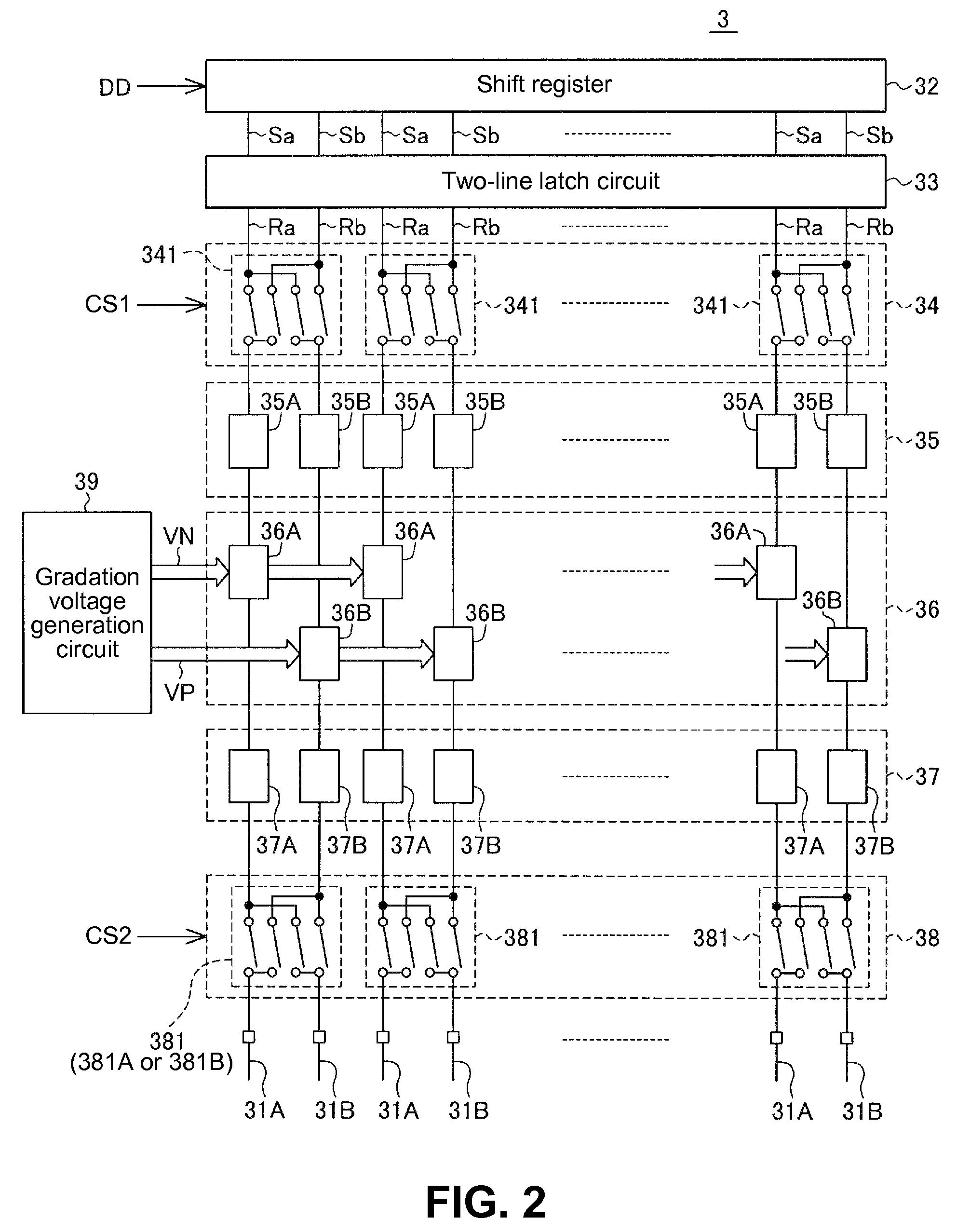
[0042]As shown in FIG. 1, the data lines 31A are situated at even-number positions, and the data lines 31B are situated at odd-number positions. Display pixels DP are disposed at cross sections of the scannin...
second embodiment
[0092]A second embodiment of the present invention will be explained next. In the second embodiment, the liquid crystal display device 1 has a configuration similar to those of the liquid crystal display device 1 in the first embodiment, except a configuration of the switch circuit 381 of the source driver 3 and a control signal supplied to the switch circuit 381.
[0093]FIG. 8 is a circuit diagram showing the switch circuit 381 (381B) of the source driver 3 of the liquid crystal display device 1 according to the second embodiment of the present invention.
[0094]As shown in FIG. 8, the switch circuit 381A includes an MOS switch SW11, an MOS switch SW12, an MOS switch SW13, and an MOS switch SW14. The MOS switch SW11 is formed of a pair of a PMOS transistor P1 and an NMOS transistor N1 connected in parallel with each other. The MOS switch SW12 is formed of a pair of a PMOS transistor P2 and an NMOS transistor N2 connected in parallel with each other. The MOS switch SW13 is formed of a p...
third embodiment
[0119]A third embodiment of the present invention will be explained next. In the third embodiment, the liquid crystal display device 1 has a configuration similar to those of the liquid crystal display device 1 in the second embodiment, except a control signal supplied to the switch circuit 381B of the source driver 3.
[0120]FIGS. 10(A) to 10(J) are timing charts showing a control operation of the source driver 3 of the liquid crystal display device 1 when the switch circuit 381B is switched between the straight connection and the cross connection according to the third embodiment of the present invention.
[0121]As shown in FIGS. 10(D) and 10(E), after the timing t1, when the switch circuit 381A is switched from the straight connection to the cross connection, after the controller 5 maintains the gate voltage Vn2 of the NMOS transistor N2 at the upper limit of the voltage range Δn (=VMM+Vnt) for a specific period of time, the controller 5 switches the gate voltage Vn2 to the power sou...
PUM
 Abstract
Description
Claims
Application Information
 - R&D
- Intellectual Property
- Life Sciences
- Materials
- Tech Scout
- Unparalleled Data Quality
- Higher Quality Content
- 60% Fewer Hallucinations
Browse by: Latest US Patents, China's latest patents, Technical Efficacy Thesaurus, Application Domain, Technology Topic, Popular Technical Reports.
© 2025 PatSnap. All rights reserved.Legal|Privacy policy|Modern Slavery Act Transparency Statement|Sitemap|About US| Contact US: help@patsnap.com