Light emitting device with transmissive film patterned in a stepwise shape and method of manufacturing the light emitting device

a technology of transmissive film and light emitting device, which is applied in the manufacture of electrode systems, electric discharge tubes/lamps, and discharge tubes luminescent screens, etc., and can solve problems such as small aperture area, large current flow, and easy step difference around pixels

Active Publication Date: 2014-08-19
SEIKO EPSON CORP
View PDF17 Cites 1 Cited by
  • Summary
  • Abstract
  • Description
  • Claims
  • Application Information

AI Technical Summary

Benefits of technology

[0008]An advantage of some aspects of the invention is to provide a top emission-type light emitting device in which a white organic EL element and a resonant structure are combined, which suppresses a decrease of the aperture area, while preventing a current from excessively flowing in the organic EL element, and the step breakage of the organic EL element and the second electrode.

Problems solved by technology

Accordingly, in this type, a step difference easily occurs around pixels, and a current excessively flows, since the thickness of film of the organic EL element becomes thin around the pixels.
In addition, if the step difference of the transparent film and the transparent conductive film is excessively high, there have been cases where the step breakage of the organic EL element and the second electrode which is formed on the organic EL element occurs.
However, there was a problem in that if the pattern position of the transparent film or the transparent conductive film is deviated in the stepwise shape as described above, and further the insulating film is formed, an aperture area becomes small by the deviation of the pattern position.

Method used


Image

  • Light emitting device with transmissive film patterned in a stepwise shape and method of manufacturing the light emitting device
  • Light emitting device with transmissive film patterned in a stepwise shape and method of manufacturing the light emitting device
  • Light emitting device with transmissive film patterned in a stepwise shape and method of manufacturing the light emitting device

Examples


application example

B: Application Example

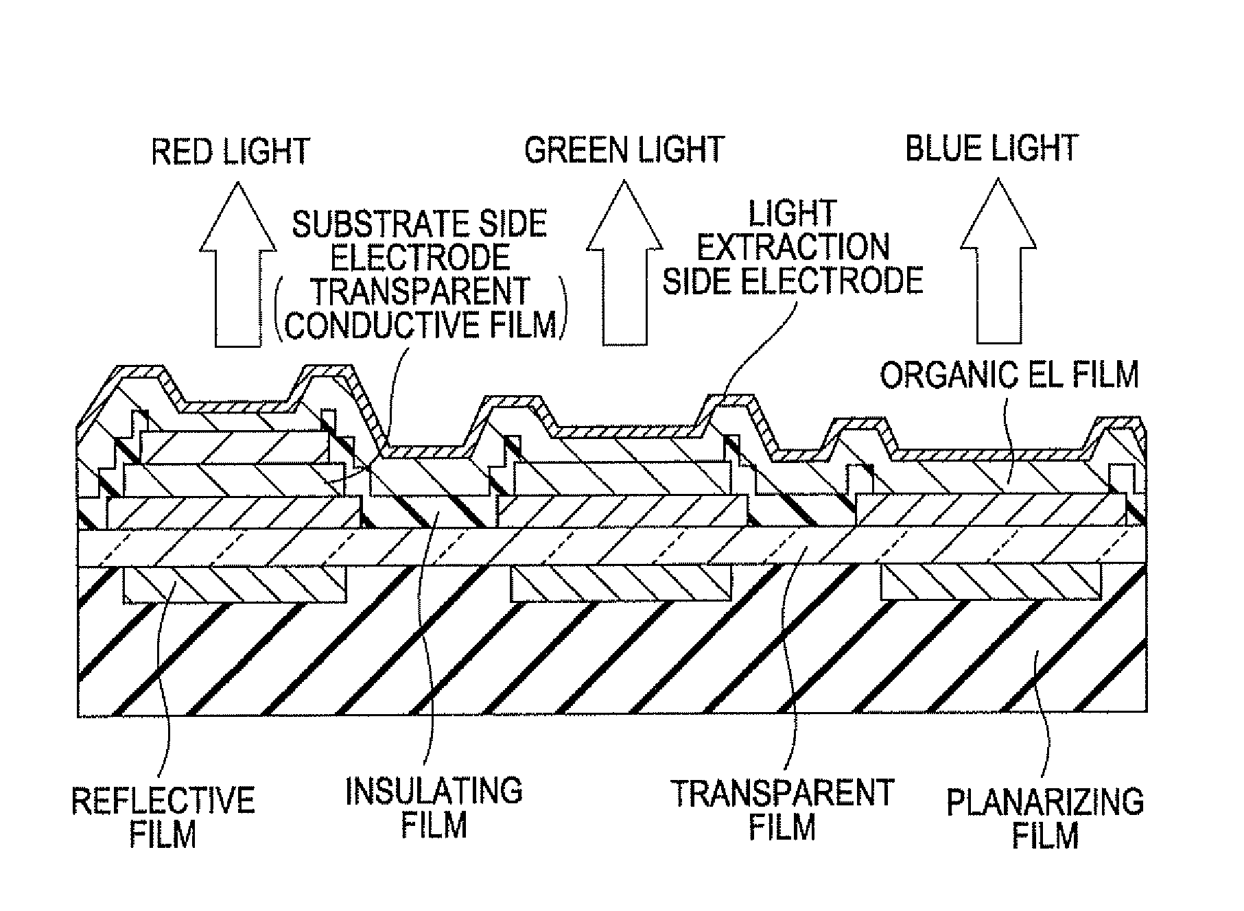
[0070]FIG. 13 is a diagram which shows a structure of a light emitting device of an application example according to the embodiment of the invention. As shown in FIG. 13, transparent conductive films may be formed in a stepwise shape by deviating a pattern position on both short sides of the light emitting element, and formed in a pattern position where the end surface is aligned in other sides.

[0071]In a high definition organic EL display in which the minimum feature size and pixel pitch of the light emitting element are similar to each other, the panel size is also small, and for example, is equal to or smaller than 1 inch. Accordingly, the resistance value for the light extraction side electrode is enough with the resistance value of metal film of about 10 nm, and for example, is 10 to 50Ω / □. For this reason, it is considered that an auxiliary wiring is not necessary. However, in the above described light emitting device according to the embodiment, the cond...


PUM


Abstract

On one short side of a rectangular aperture area, transparent conductive films are patterned by being deviated in a stepwise shape. On another side, an end surface of the transparent conductive films is patterned to be aligned. The end surface of the transparent conductive films is covered with an insulating film.

Description

BACKGROUND[0001]1. Technical Field[0002]The present invention relates to a light emitting device in which various light emitting elements are used, and a method of manufacturing the light emitting device.[0003]2. Related Art[0004]In recent years, a top emission-type light emitting device has been widely used as a display device of an electronic apparatus, which forms an organic EL (electroluminescence) element on a substrate as a light emitting element, and extracts emission light of the light emitting element to the opposite side of the substrate. In the top emission-type, a reflecting layer is formed between a first electrode (for example, an anode) on one side on which the light emitting element is inserted, and which is formed on a substrate side, and the substrate, and light is extracted from a second electrode (for example, a cathode) on another side on which the light emitting is inserted, and of which a light use efficiency is high.[0005]In addition, a technology is disclose...

Claims


Application Information

Patent Timeline
Patent Type & Authority Patents(United States)
IPC IPC(8): H01J1/62H01J9/00H01L27/32H01L51/52H05B33/00
CPCH01L51/5265H01L27/3216H01L2251/5315H10K59/352H10K50/852H10K2102/3026
Inventor SHIRATORI, KOYA
Owner SEIKO EPSON CORP
Why Eureka
Try Eureka