
Semiconductor memory device and test method therefor

a memory device and semiconductor technology, applied in the direction of information storage, static storage, digital storage, etc., can solve the problems of increasing the deviation of the snm, excessive operation margin, and more difficult to secure the operation margin, and achieve excellent productivity

Inactive Publication Date: 2012-10-09
RENESAS ELECTRONICS CORP
View PDF8 Cites 0 Cited by
  • Summary
  • Abstract
  • Description
  • Claims
  • Application Information

AI Technical Summary

Benefits of technology

[0010]The evaluation of the operation margin using the SNM is suitable as long as the number of rows is large and the deviation between the SNM and DNM is small as in the conventional case. However, when the number of rows is reduced, as described above, the deviation between the SNM and DNM increases. Accordingly, the evaluation of the operation margin using the SNM has a problem in that the operation margin becomes excessively large and the yield is considerably lowered. In other words, if the operation margin can be evaluated appropriately by using the DNM, the yield, i.e., the productivity of high-speed SRAMs can be improved.
[0013]The provision of the controller that controls the first switch circuit to render the first bit line pair and the second bit line pair conductive, in the case of testing the first SRAM cell, makes it possible to provide a semiconductor memory device which is capable of evaluating the operation margin simply by using the DNM and is excellent in the productivity based on the DNM evaluation.
[0014]According to an exemplary aspect of the present invention, it is possible to provide a semiconductor memory device excellent in the productivity based on the evaluation of the operation margin using the DNM.

Problems solved by technology

The recent miniaturization of static random access memories (SRAMs) has made it more difficult to secure their operation margin.
Meanwhile, the DNM is a dynamic evaluation value which rapidly decreases as the number of rows decreases, resulting in an increase in deviation from the SNM.
Accordingly, the evaluation of the operation margin using the SNM has a problem in that the operation margin becomes excessively large and the yield is considerably lowered.

Method used


Image

  • Semiconductor memory device and test method therefor
  • Semiconductor memory device and test method therefor
  • Semiconductor memory device and test method therefor

Examples


first exemplary embodiment

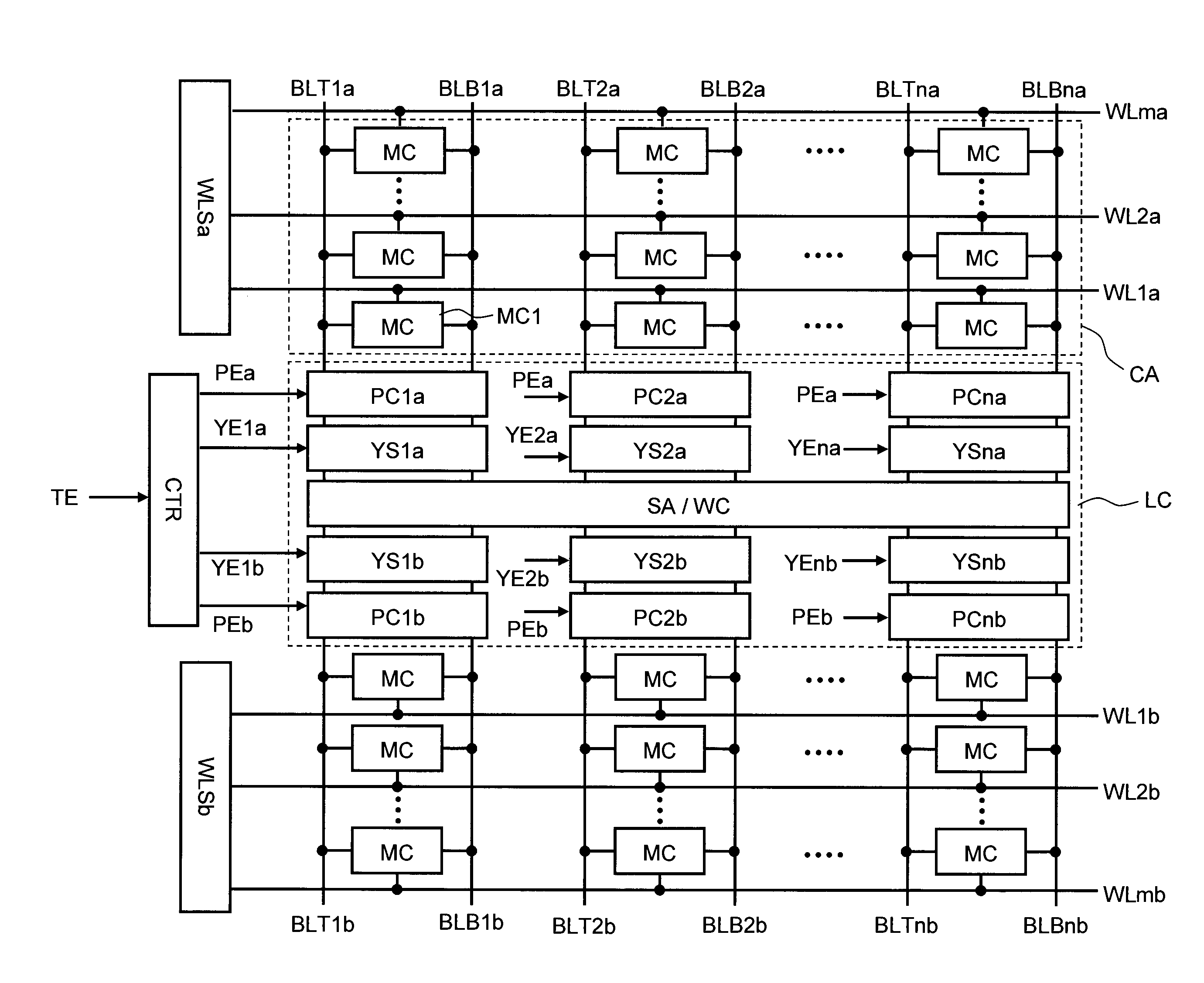
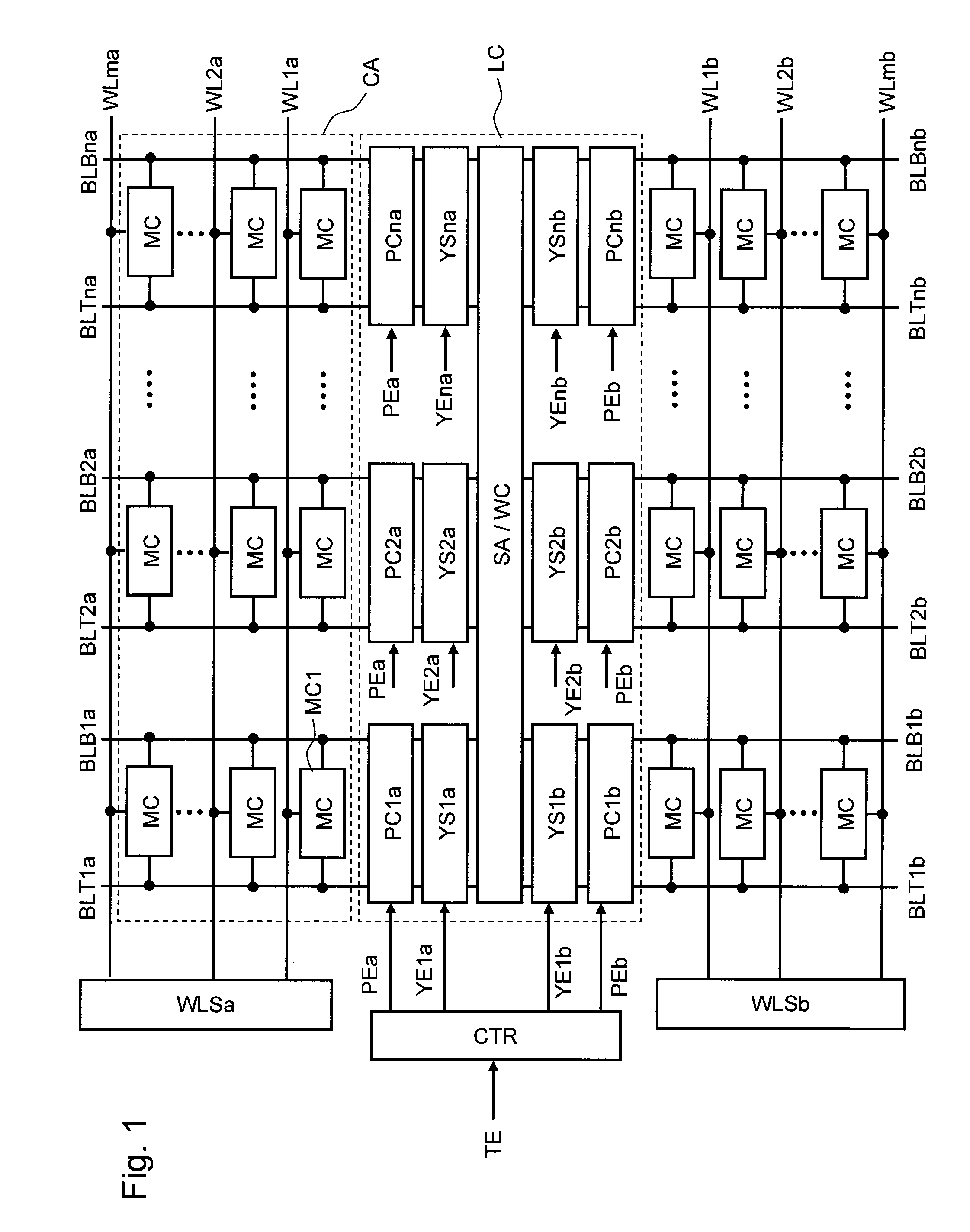
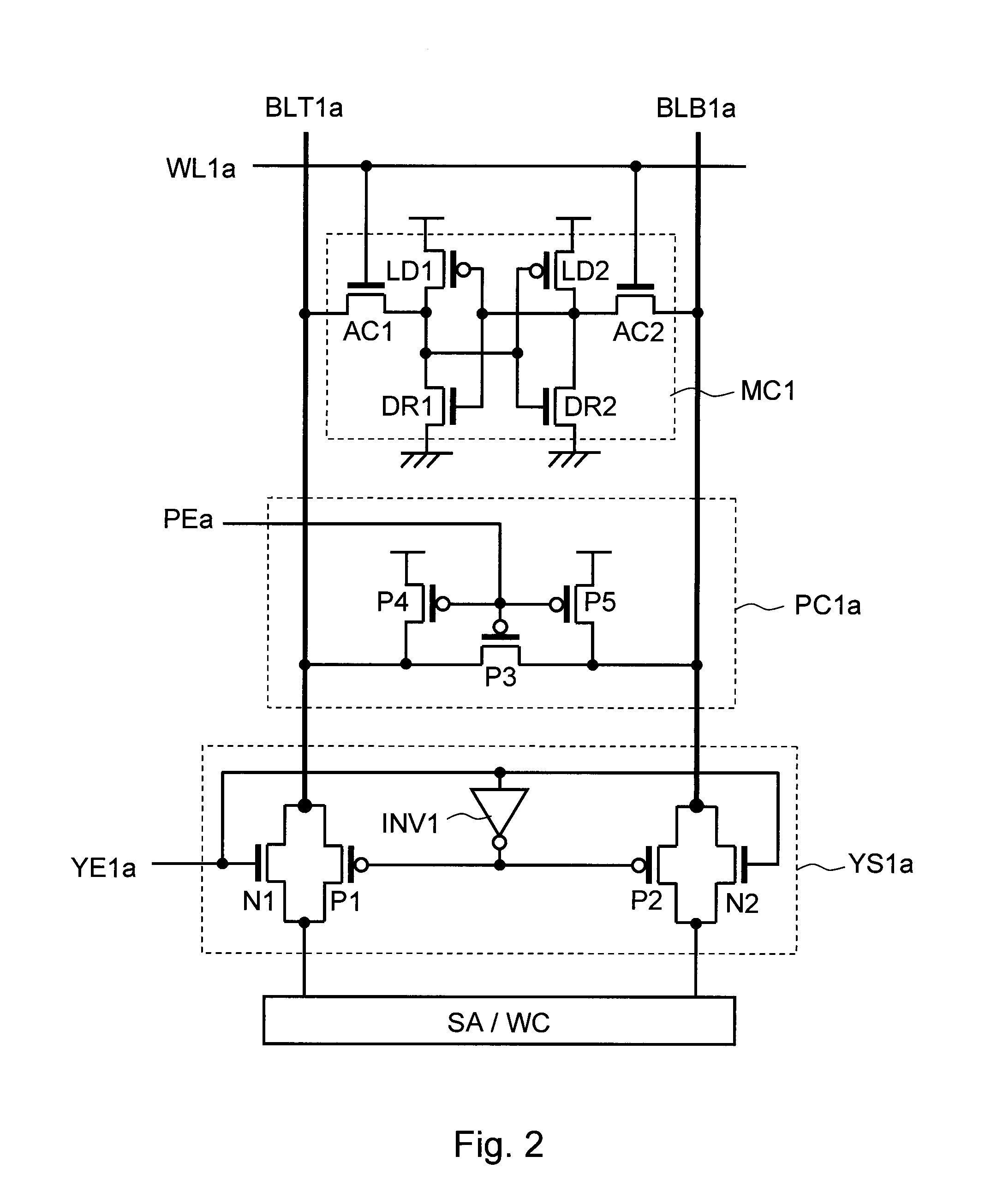
[0031]FIG. 1 is a circuit diagram illustrating a semiconductor memory device according to a first exemplary embodiment of the present invention. The semiconductor memory device is an SRAM. The semiconductor memory device includes a control circuit CTR, a sense amplifier SA, a write circuit WC, n (n is a natural number) pairs of Y selectors YS1a to YSna and YS1b to YSnb, n pairs of precharge circuits PC1a to PCna and PC1b to PCnb, 2n pairs of bit lines BLT1a and BLB1a to BLTna and BLBna, and BLT1b and BLB1b to BLTnb and BLBnb, a pair of word line selectors WLSa and WLSb, m (m is a natural number) pairs of word lines WL1a to WLma and WL1b to WLmb, and n×m pairs of memory cells MC. The sense amplifier and write circuit SA / WC includes the sense amplifier SA and the write circuit WC which are integrally illustrated in FIG. 1 for convenience of illustration. The sense amplifier SA is a circuit that amplifies a potential difference between two sense nodes of a memory cell MC selected in a ...

second exemplary embodiment

[0066]Next, a second exemplary embodiment of the present invention will be described with reference to FIG. 8. FIG. 8 is a circuit diagram illustrating a semiconductor memory device according to the second exemplary embodiment. The semiconductor memory device shown in FIG. 8 differs from the semiconductor memory device shown in FIG. 1 in that bridge circuits BLG for connecting the bit line pairs which are opposed to each other through the local circuit LC are provided for each bit line pair. The other configurations are similar to those of the first exemplary embodiment, so the description thereof is omitted.

[0067]Specifically, the bit line pair BLT1a and BLB1a and the bit line pair BLT1b and BLB1b are connected through the bridge circuit BLG without involving the sense amplifier SA. That is, between the bit line pair BLT1a and BLB1a and the bit line pair BLT1b and BLB1b, the bridge circuit BLG and the sense amplifier SA are connected in parallel with each other. Similarly, a bit li...

third exemplary embodiment

[0071]Next, a third exemplary embodiment of the present invention will be described with reference to FIG. 10. FIG. 10 is a circuit diagram illustrating a semiconductor memory device according to the third exemplary embodiment. The semiconductor memory device shown in FIG. 10 includes two circuits shown in FIG. 1, and the two circuits are connected through the bridge circuits BLG.

[0072]On both sides of the local circuit LC1, cell arrays CAa and CAb are connected to each other. Similarly, on both sides of the local circuit LC2, cell arrays CAc and CAd are connected to each other. Additionally, word line selectors WLSb, WLSc, and WLSd are connected to the cell arrays CAb, CAc, and CAd through word lines WLb, WLc, WLd, respectively. Note that the word lines WLb, WLc, and WLd are each represented by one line for convenience of illustration. The detailed configurations of the local circuits LC1 and LC2 and the cell arrays CAa, CAb, CAc, and CAd are similar to those of FIG. 1.

[0073]The ce...


PUM


Abstract

Provided is a semiconductor memory device including: first and second SRAM cells; a first bit line pair provided with the first SRAM cell; a second bit line pair provided with the second SRAM cell; a first switch circuit provided between the first bit line pair and the second bit line pair; and a controller that controls the first switch circuit to render the first bit line pair and the second bit line pair conductive, in a case of testing the first SRAM cell.

Description

INCORPORATION BY REFERENCE[0001]This application is based upon and claims the benefit of priority from Japanese patent application No. 2009-045330, filed on Feb. 27, 2009, the disclosure of which is incorporated herein in its entirety by reference.BACKGROUND[0002]1. Field of the Invention[0003]The present invention relates to a semiconductor memory device and a test method therefor, and more particularly, to a static random access memory (SRAM) and a test method therefor.[0004]2. Description of Related Art[0005]The recent miniaturization of static random access memories (SRAMs) has made it more difficult to secure their operation margin. As disclosed in Japanese Unexamined Patent Application Publication No. 2007-102902 and Published Japanese Translation of PCT International Publication for Patent Application, No. 2008-522334 (PCT Application WO 2006 / 056902), the operation margin of SRAMs is generally evaluated using static noise margin (SNM). In contrast to the SNM, dynamic noise ma...

Claims


Application Information

Patent Timeline
Patent Type & Authority Patents(United States)
IPC IPC(8): G11C11/00G11C7/00G11C29/00
CPCG11C29/50G11C11/41G11C2029/5002G11C2029/1204
Inventor ASAYAMA, SHINOBU
Owner RENESAS ELECTRONICS CORP
Learn More