
Nanostructured dielectric materials for high energy density multi layer ceramic capacitors

a ceramic capacitor and nanostructured dielectric technology, applied in the field of ceramic science, can solve the problems of high dielectric loss and lower resistivity of devices, and achieve the effect of high energy density capacitors

Active Publication Date: 2012-09-11
UNIVERSITY OF MISSOURI
View PDF12 Cites 10 Cited by
  • Summary
  • Abstract
  • Description
  • Claims
  • Application Information

AI Technical Summary

Benefits of technology

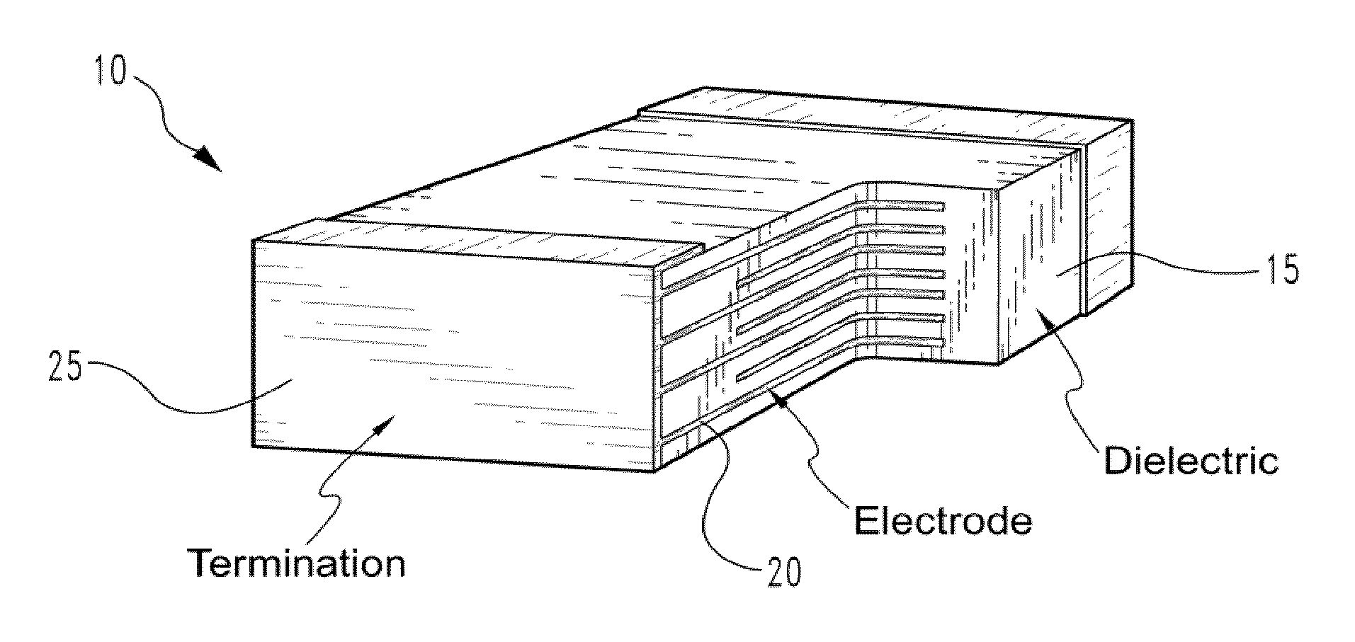
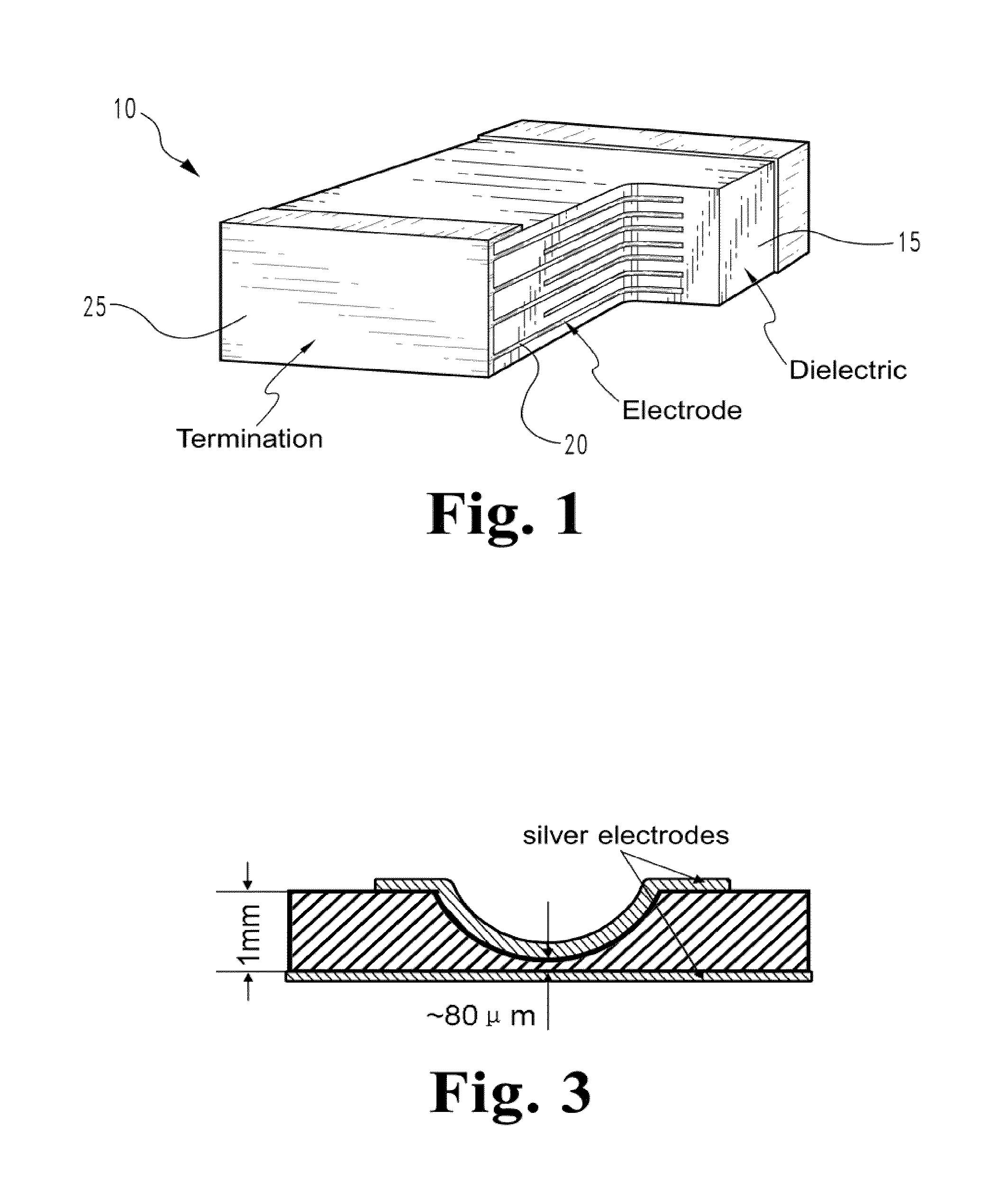
The invention describes a new ceramic material that can be used in high energy density capacitors. This material has very small grain sizes and no holes or gaps, making it more dense and better suited for use in capacitors. The method for making this material involves compacting a ceramic powder and then sintering it in an oxidizing atmosphere. The resulting material has a high energy density, meaning it can store more energy than other materials. The invention also describes a high energy density capacitor made using this new ceramic material.

Problems solved by technology

However, thus far pure TiO2 nanopowder material has seldom been used as a dielectric material for capacitor applications as it can easily be reduced, leading to devices having lower resistivity and high dielectric loss, even though the intrinsic dielectric loss of stoichiometric TiO2is very low.

Method used


Image

  • Nanostructured dielectric materials for high energy density multi layer ceramic capacitors
  • Nanostructured dielectric materials for high energy density multi layer ceramic capacitors
  • Nanostructured dielectric materials for high energy density multi layer ceramic capacitors

Examples


examples

I Microstructural Developments and General Testing Conditions

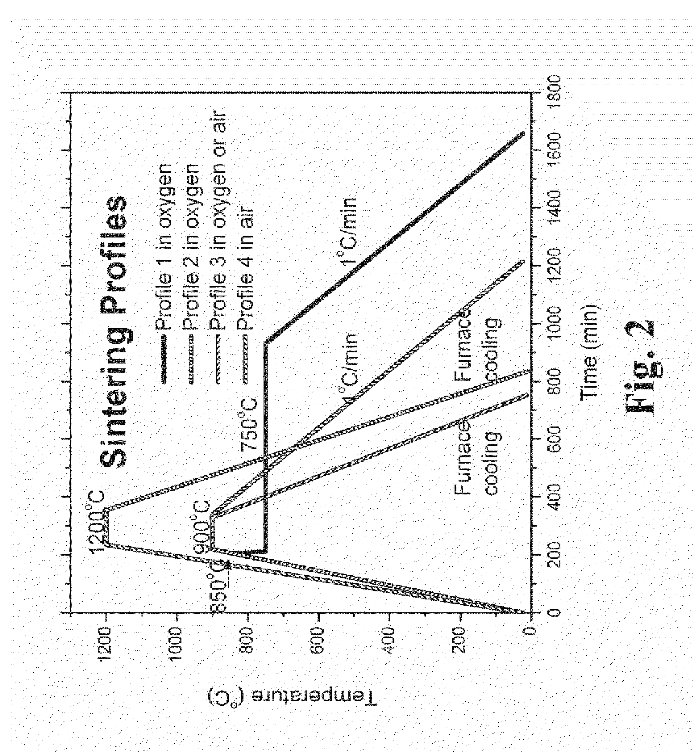
[0038]NANOTEK® TiO2 powders were obtained as starting materials for MLCC production, with powder characteristics and main impurity levels reproduced from the included product data sheet as Tables 1 and 2, respectively (NANOTEK is a registered trademark of Nanophase Technologies Corporation, 1319 Marquette Drive, Romeoville, Ill., 60446, Reg. No. 1978354). Green compacts were prepared by uniaxial pressing at 50 MPa and subsequent cold isostatic pressing at 300 MPa. Sintering was conducted at various temperatures (750° C.-1200° C.) in pure oxygen (1 atm.) or air with different cooling rates (furnace cooling or 1° C. / min cooling rate).

[0039]

TABLE 1Characteristics of the starting powdersCharacteristicsValuePurity99.9%Average particle size (nm)40Specific surface area (m2 / g)38Bulk density (g / cm3)0.20True density (g / cm3)3.95Crystal phase80% anatase and 20% rutile

[0040]

TABLE 2Main impurities in the TiO2 powderElementsImpurity leve...


PUM

PropertyMeasurementUnit
thicknessaaaaaaaaaa
diameteraaaaaaaaaa
grain sizeaaaaaaaaaa

Abstract

A high energy density multilayer ceramic capacitor, having at least two electrode layers and at least one substantially dense polycrystalline dielectric layer positioned therebetween. The at polycrystalline dielectric layer has an average grain size of less than about 300 nanometers, a particle size distribution of between about 150 nanometers and about 3 micrometers, and a maximum porosity of about 1 percent. The dielectric layer is selected from the group including TiO2, BaTiO3, Al2O3, ZrO2, lead zirconium titanate, and combinations thereof and has a breakdown strength of at least about 1100 kV per centimeter.

Description

GRANT STATEMENT[0001]The invention was made in part from government support under Grant No. RG001083 from the National Science Foundation (NSF / IUCRC Center for Dielectric Studies) and under Grant No. N000-14-05-1-0541 from the Office of Naval Research. The U.S. Government has certain rights in the invention.TECHNICAL FIELD[0002]The present invention relates to the field of ceramic science and, more particularly high energy density multilayer ceramic capacitors.BACKGROUND[0003]Titanium dioxide (TiO2) is one of the most widely used ceramic materials, having a broad range of applications such as pigments, sensors, waste treatment, solar cells and capacitors. Nanocrystalline TiO2 ceramics have been the subject of great interest to researchers over the years. Research has been conducted in such diverse areas as TiO2 nanopowder synthesis, thin film fabrication, and the sintering of bulk ceramics. However, thus far pure TiO2 nanopowder material has seldom been used as a dielectric material...

Claims


Application Information

Patent Timeline
Patent Type & Authority Patents(United States)
IPC IPC(8): C04B35/46C04B35/111C04B35/468
CPCB82Y30/00C04B35/486C04B35/111H01G4/1209C04B35/491C04B35/4682C04B35/46H01G4/1281H01G4/30Y10T428/266C04B2235/782C04B2235/6565C04B2235/785C04B2235/781C04B2235/85
Inventor DOGAN, FATIH
Owner UNIVERSITY OF MISSOURI
Learn More