
Magnetic random access memory

a random access and memory technology, applied in the field of magnetic random access memory, can solve problems such as the complexity of the structure of the magnetoresistance element, and achieve the effect of suppressing the variation in the reference level, improving the write characteristics and read characteristics

Active Publication Date: 2012-04-17
NEC CORP
View PDF13 Cites 8 Cited by
  • Summary
  • Abstract
  • Description
  • Claims
  • Application Information

AI Technical Summary

Benefits of technology

This approach effectively reduces the write threshold current density while enhancing the read-out signal and stabilizing the reference level, thereby improving the reliability and accuracy of data reading in MRAM.

Problems solved by technology

In this case, however, a structure of the magnetoresistance element becomes complicated, which is likely to increase variation in magnetization state between memory cells in which the same data value is stored.

Method used


Image

  • Magnetic random access memory
  • Magnetic random access memory
  • Magnetic random access memory

Examples


Embodiment Construction

[0066]A magnetoresistance element and an MRAM based on the spin transfer magnetization switching method according to an exemplary embodiment of the present invention will be described with reference to the attached drawings.

[0067]1. First Magnetoresistance Element

[0068]1-1. Configuration

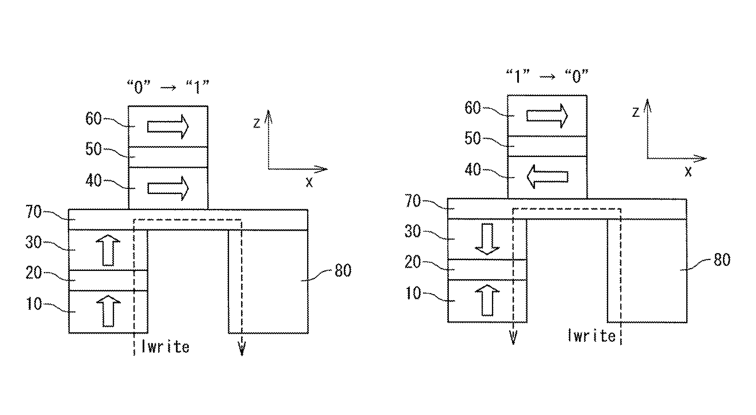
[0069]FIG. 1A is a perspective view showing a structure of a first magnetoresistance element 1 according to an exemplary embodiment of the present invention. FIG. 1B and FIG. 1C respectively are a x-y plan view and a x-z side view of the structure shown in FIG. 1A. The first magnetoresistance element 3 has a stacked structure including a plurality of layers, and the stack direction is defined as the z-axis direction. A plane parallel to each layer of the stacked structure is the x-y plane.

[0070]The first magnetoresistance element 1 according to the present exemplary embodiment has a first magnetization fixed layer 10, a first spacer layer 20, a first magnetization free layer 30, a second magnetizatio...


PUM


Abstract

An MRAM has: a memory cell including a first magnetoresistance element; and a reference cell including a second magnetoresistance element. The first magnetoresistance element has a first magnetization fixed layer, a first magnetization free layer, a first nonmagnetic layer sandwiched between the first magnetization fixed layer and the first magnetization free layer, a second magnetization fixed layer, a second magnetization free layer and a second nonmagnetic layer sandwiched between the second magnetization fixed layer and the second magnetization free layer. The first magnetization fixed layer and the first magnetization free layer have perpendicular magnetic anisotropy, and the second magnetization fixed layer and the second magnetization free layer have in-plane magnetic anisotropy. The first magnetization free layer and the second magnetization free layer are magnetically coupled to each other. Center of the second magnetization free layer is displaced in a first direction from center of the first magnetization free layer in a plane parallel to each layer. Whereas, the second magnetoresistance element has: a third magnetization free layer whose magnetization easy axis is parallel to a second direction; a third magnetization fixed layer whose magnetization direction is fixed in a third direction perpendicular to the second direction; and a third nonmagnetic layer sandwiched between the third magnetization fixed layer and the third magnetization free layer. The third magnetization fixed layer and the third magnetization free layer have in-plane magnetic anisotropy.

Description

[0001]This application is the National Phase of PCT / JP2009 / 050185, filed Jan. 9, 2009 which is based upon and claims the benefit of priority from Japanese patent application No. 2008-038067, filed on Feb. 19, 2008, the disclosure of which is incorporated herein in its entirely by reference.TECHNICAL FIELD[0002]The present invention relates to a magnetic random access memory (MRAM: Magnetic Random Access Memory). In particular, the present invention relates to an MRAM based on spin transfer magnetization switching method.BACKGROUND ART[0003]An MRAM is a nonvolatile random access memory that utilizes a magnetoresistance element such as a magnetic tunnel junction (Magnetic Tunnel Junction; MTJ) element as a memory element. Since the MRAM is capable of achieving high-speed operation and can have infinite rewrite tolerance, research and development of the MRAM have been actively carried out to achieve commercialization in recent years. To further improve the versatility of the MRAM herea...

Claims


Application Information

Patent Timeline
Patent Type & Authority Patents(United States)
IPC IPC(8): G11C11/15
CPCG11C11/16H01L27/222H01L43/08Y10S977/933Y10S977/935G11C11/1655G11C11/1659G11C11/161G11C11/1673G11C11/1675H10B61/00H10N50/10
Inventor FUKAMI, SHUNSUKEISHIWATA, NOBUYUKISUZUKI, TETSUHIROOHSHIMA, NORIKAZUNAGAHARA, KIYOKAZU
Owner NEC CORP
Learn More