Electrostatic chuck and electrode sheet for electrostatic chuck

a technology of electrostatic chuck and electrode sheet, which is applied in the direction of electrostatic holding device, electrical apparatus, thin material handling, etc., can solve the problems of increasing the amount of ions implanted to the silicon wafer per unit time, increasing the substrate temperature of the silicon wafer or the like, and achieving excellent chucking force, excellent holding force, and efficient generation of gradient force

Inactive Publication Date: 2012-04-17
CREATIVE TECH CORP
View PDF14 Cites 2 Cited by
  • Summary
  • Abstract
  • Description
  • Claims
  • Application Information

AI Technical Summary

Benefits of technology

[0030]According to the present invention, the shape of the pattern electrode forming the second electrode layer is specified, so the penetration potential from the first electrode layer, which is distributed on the sample chucking surface side can be optimized. Therefore, it is possible to obtain the electrostatic chuck which efficiently generates the gradient force on the sample chucking surface to exercise the excellent chucking force and the excellent holding force. In the electrostatic chuck according to the present invention, the second electrode layer located on the sample chucking surface side includes the pattern electrode having the predetermined opening portions, so a Coulomb force acts in addition to the gradient force. Therefore, the excellent chucking force and the excellent holding force can be exercised to any one of a semiconductor substrate such as a silicon wafer and an insulating substrate such as a glass substrate. Such an electrostatic chuck is sufficiently adaptable to the requirement for an increase in size of the held substrate. Further, the contact characteristic of the substrate to the sample chucking surface can be improved, so the substrate can be efficiently cooled.

Problems solved by technology

However, an increase in an ion beam current has let to a problem in which the amount of ions implanted to a silicon wafer per unit time increases and the cooling performance of the electrostatic chuck for cooling the silicon wafer cannot sufficiently accommodate the increase.
However, a substrate temperature of the silicon wafer or the like tends to increase with an increase in amount of ions implanted and there are causes such as inherent warp or distortion of the substrate and the poor flatness of the sample chucking surface, so there is a problem that the substrate cannot be brought into sufficient contact with the sample chucking surface and thus the substrate is not cooled as much.
However, when the substrate is not sufficiently cooled, the temperature thereof exceeds a heat resistance temperature of the resist film.
Therefore, the resist film is hardened, so it is difficult to remove the resist film from the substrate.
Thus, subsequent processes may be affected.
With an increase in size of a silicon wafer or a substrate made of glass or the like, a problem with respect to the cooling of the substrate becomes more significant.
However, when the distance between the adjacent electrodes is further narrowed, it is likely to cause a discharge between the electrodes.
Therefore, it is difficult to apply a sufficient chucking force to particularly a large substrate.
However, up to now, such a type of electrostatic chuck is not sufficiently studied in view of the effective exercise of the gradient force.Patent Document 1: JP 10-223742 APatent Document 2: JP 2000-502509 APatent Document 3: JP 2005-64105 APatent Document 4: JP 2003-243493 A

Method used


Image

  • Electrostatic chuck and electrode sheet for electrostatic chuck
  • Electrostatic chuck and electrode sheet for electrostatic chuck
  • Electrostatic chuck and electrode sheet for electrostatic chuck

Examples


first embodiment

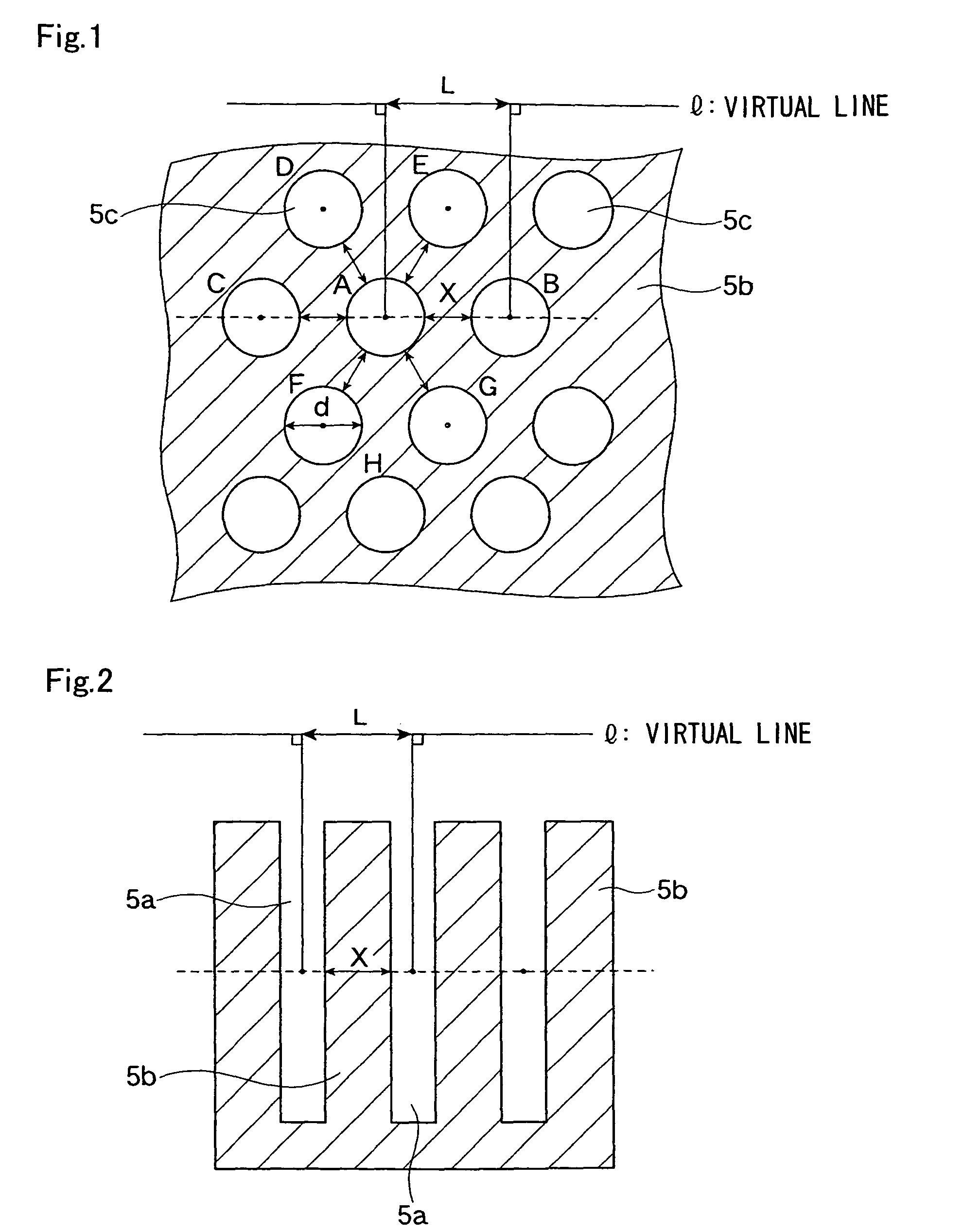
[0056]FIG. 3 is an explanatory exploded perspective view showing a bipolar electrostatic chuck X according to a first embodiment.FIG. 4 is an explanatory view showing a part of a cross-section A-A′ of the bipolar electrostatic chuck X shown in FIG. 3. A polyimide sheet which is 206 mm long and 206 mm wide is employed in which a copper surface layer having a film thickness of 12 μm is provided on a surface of a polyimide layer (name of product manufactured by Mitsui Chemicals, Inc.: NEOFLEX). The polyimide layer (50 μm in film thickness and 3.5 in dielectric constant) is provided as the interelectrode insulating layer 4. An outer edge of the copper surface layer is removed by etching to form the first electrode layer 3 (200 mm long and 200 mm wide) in which the entire flat area corresponds to the conductive portion. A chromium film is deposited at 0.1 μm on the surface of the polyimide layer (interelectrode insulating layer 4) of the polyimide sheet and a copper film whose film thick...

second embodiment

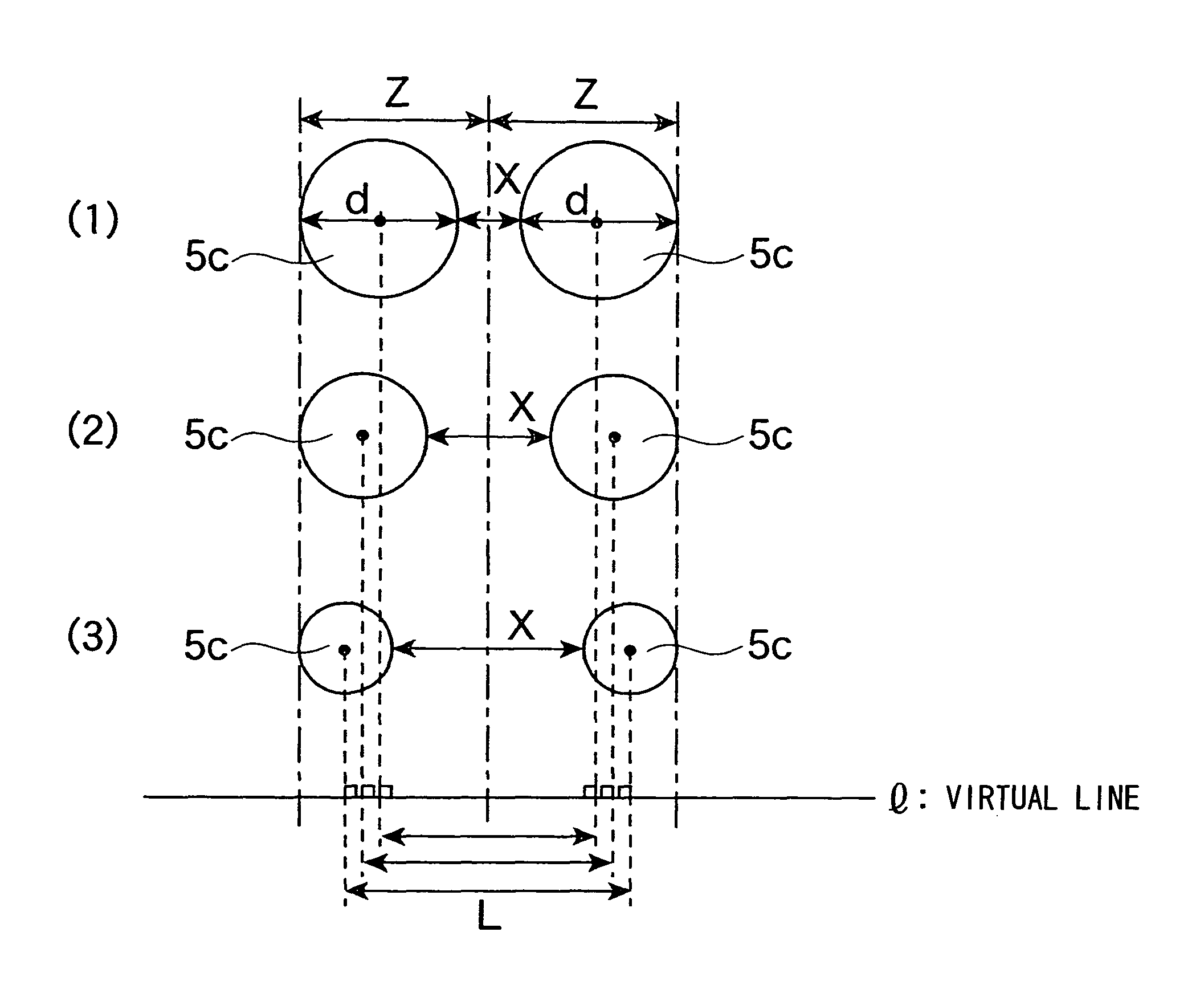
[0059]The polyimide sheet (name of product manufactured by Mitsui Chemicals, Inc.: NEOFLEX) is used as in the case of the first embodiment and cut off at a diameter of 184 mm. The polyimide layer is provided as the interelectrode insulating layer 4. The outer edge of the copper surface layer is removed by etching to form the first electrode layer 3 having a diameter of 182 mm in which the entire flat area corresponds to the conductive portion. A chromium film is deposited at 0.1 μm on the surface of the polyimide layer (interelectrode insulating layer 4) of the polyimide sheet and a copper film whose film thickness is 0.4 μm is formed on the chromium film by an ion plating method. Then, predetermined mask processing and etching processing are performed. As a result, as shown in FIG. 1, the pattern electrode having the mesh-shaped conductive portion 5b in which the plurality of circular holes 5c each having a diameter d of 1.2 mm are provided is formed. The pattern electrode is used ...


PUM

PropertyMeasurementUnit
distanceaaaaaaaaaa
distanceaaaaaaaaaa
thicknessaaaaaaaaaa

Abstract

An electrostatic chuck having excellent chucking force and holding force is provided. The electrostatic chuck includes a laminate structure in which a first insulating layer, a first electrode layer, an interelectrode insulating layer, a second electrode layer and a second insulating layer are successively laminated on a metal base in an order of increasing distance from the metal base. The second electrode layer includes a pattern electrode having a plurality of opening portions within a flat area, and a shortest distance X between mutually opening portions and a length L of a line segment formed by feet of perpendiculars when barycenters of the adjacent opening portions are projected to a virtual line which is a straight line parallel to the shortest distance X satisfy L / X≧1.5 and L<2.6 mm.

Description

TECHNICAL FIELD[0001]The present invention relates to an electrostatic chuck and an electrode sheet for the electrostatic chuck.BACKGROUND ART[0002]Electrostatic chucks are widely used in order to attract / hold a wafer made of a semiconductor such as silicon in various devices including an ion implanting device, a plasma processing device, an etching device, an electron exposure device, and an ion rendering device during a semiconductor producing process. Also, in a liquid crystal producing field, the electrostatic chucks are used in order to attract / hold a glass substrate serving as an insulating substrate in a substrate bonding device employed to press-insert a liquid crystal between the insulating substrates, an ion doping apparatus, or the like.[0003]In recent years, a panel size is becoming increasingly larger as the demand for flat panel displays grows. For example, a liquid crystal mother glass substrate having a size as large as 2 m×2 m has appeared. In order to process such ...

Claims


Application Information

Patent Timeline
Patent Type & Authority Patents(United States)
IPC IPC(8): B32B3/24H01L21/68
CPCH01L21/6831H01L21/6833H02N13/00Y10T428/24331Y10T428/24851H01L21/68H01L21/683
Inventor MIYASHITA, KINYAFUJISAWA, HIROSHIHARANO, RIICHIRO
Owner CREATIVE TECH CORP
Why Eureka
Try Eureka