Integrated structure with transistors and Schottky diodes and process for fabricating the same

a technology of integrated structure and transistor, which is applied in the direction of diodes, semiconductor devices, electrical devices, etc., can solve the problems of reduced operation speed, reduced gain, and excessive parasitic capacitance and resistance of the process, so as to minimize the physical size of the diode and the parasitic capacitance and resistance

Active Publication Date: 2011-08-02
HRL LAB
View PDF4 Cites 14 Cited by
  • Summary
  • Abstract
  • Description
  • Claims
  • Application Information

AI Technical Summary

Benefits of technology

[0018]A process for fabricating an integrated group III nitride structure comprising high electron mobility transistors (HEMTs) and Schottky diodes, and the resulting structure, are disclosed. Integration of vertical junction Schottky diodes is enabled, and the parasitic capa...

Problems solved by technology

However, the gate/source Schottky diode (one of the key components used in digital, analog or mixed-mode circuit) in the existing GaN HEMT process suffers from excessive parasitic capacitance and resistance due to its lateral junction structure, and non-ideal semiconductor layer structure.
This parasitic capacitance and resistance leads to lower operation speed, lower gain, higher power consumption, and larger physical size.
The non-ideal larger structure also leads to large and variable non-ideality factors in the Schottky diode I-V characteristics.
While the undoped layer 6 provides for high carrier mobility underneath the gate 14, the low carrier concentration leads to a high series resistance between the gate 14 and the cathode contact 7, 8, resulting in increased loss in switching and level shifting applications.
With this conventional gate Schottky structure, reductions in this resistance c...

Method used


Image

  • Integrated structure with transistors and Schottky diodes and process for fabricating the same
  • Integrated structure with transistors and Schottky diodes and process for fabricating the same
  • Integrated structure with transistors and Schottky diodes and process for fabricating the same

Examples


Embodiment Construction

[0036]FIG. 2 shows an improved process and an improved integrated Schottky structure in accordance with the present disclosure.

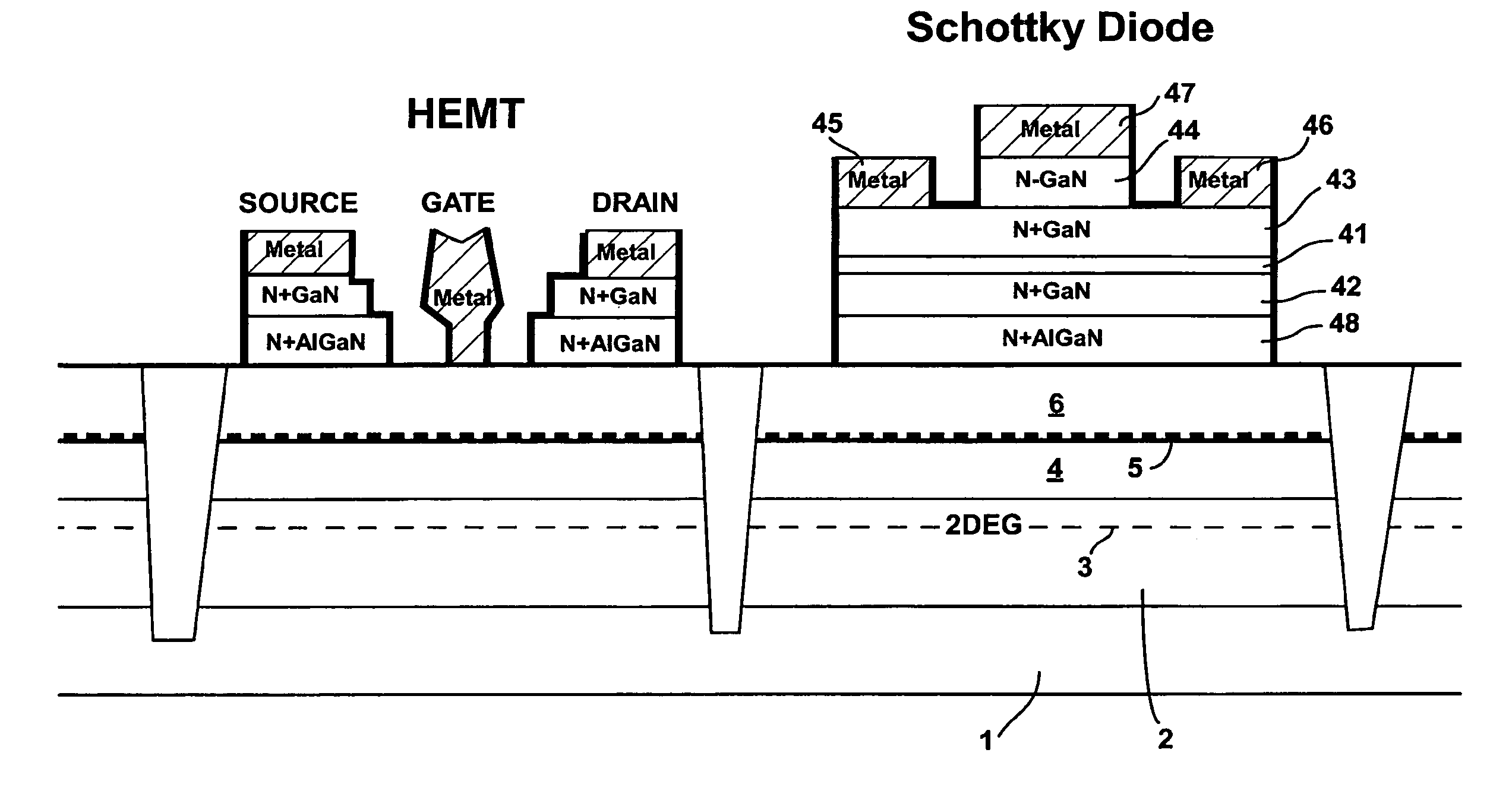
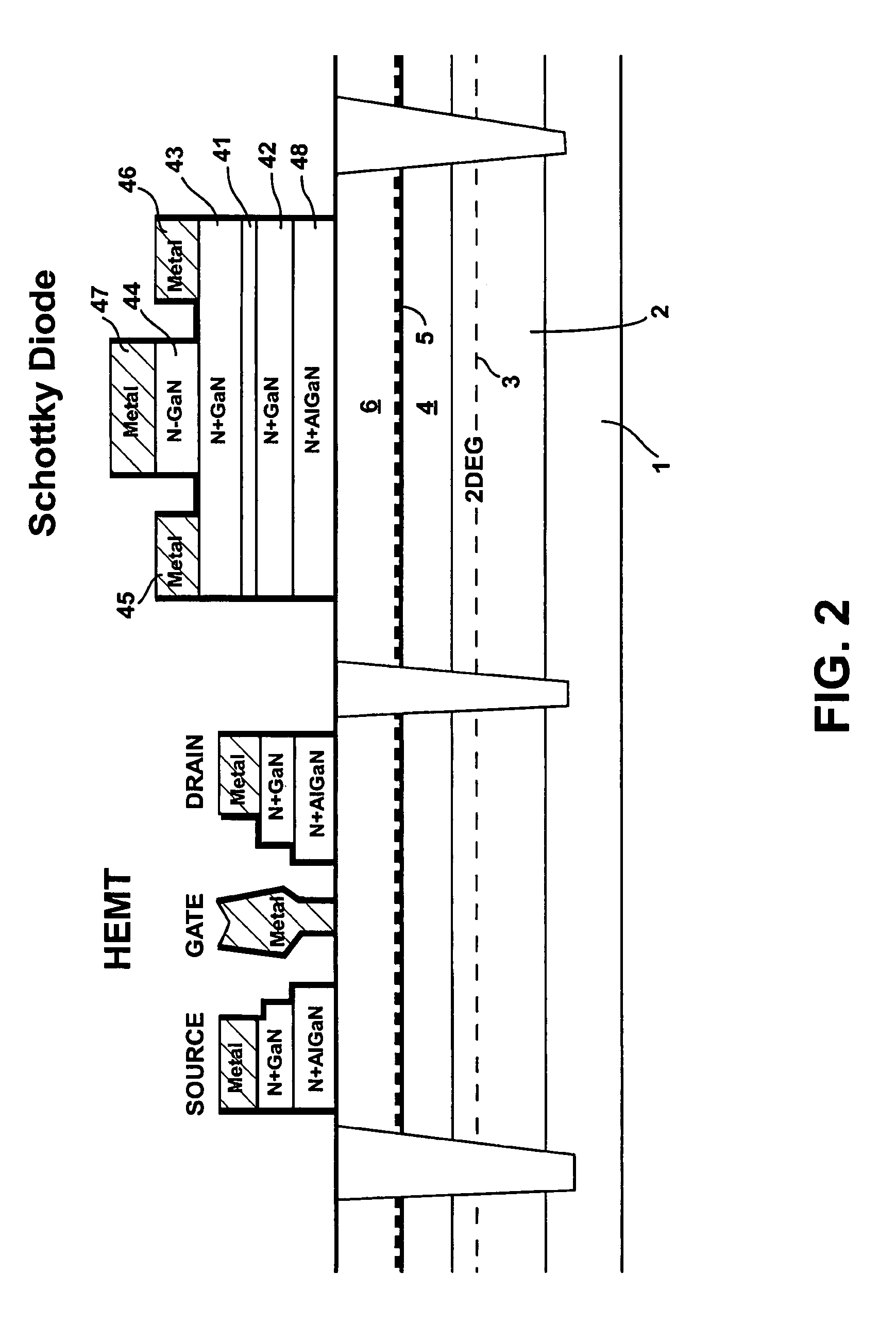
[0037]The HEMT depositing is performed as per the prior art, depositing a first intermediate layer 11, 12, 48 of N+ doped AlGaN and a second intermediate layer 9, 10, 42 of N+ GaN. An AlN etch stop layer 41 is formed above the N+ doped GaN “cap” layer 42 from which cap layers 9, 10 of the HEMT shown in FIG. 1 and on the left side of FIG. 2 are formed. A third intermediate layer, or second N+ doped GaN layer, 43 is formed on top of the AlN etch stop layer 41 to form the back side (cathode) contact to the diode. The fourth intermediate layer, an N− doped GaN layer 44 is formed in the gate region. Cathode metals 45, 46 are put on top of the second N+ doped GaN layer 43, while anode metal 47 is put above the N− doped GaN layer 44. The thickness and doping level of the N− doped GaN layer 44 are controllable and can be optimized for diode performance.

[0038]In area...


PUM


Abstract

A process for fabricating an integrated group III nitride structure comprising high electron mobility transistors (HEMTs) and Schottky diodes, and the resulting structure, are disclosed. Integration of vertical junction Schottky diodes is enabled, and the parasitic capacitance and resistance as well as the physical size of the diode are minimized. A process for fabricating an integrated group III nitride structure comprising double-heterostructure field effect transistors (DHFETs) and Schottky diodes and the resulting structure are also disclosed.

Description

BACKGROUND[0001]1. Field[0002]The present disclosure relates generally to transistors, diodes and fabrication processes for transistors and diodes. More particularly, it relates to an integrated structure comprising transistors, either high electron mobility or double-heterostructure field effect, and Schottky diodes and a process for fabricating the same.[0003]2. Description of the Related Art[0004]Gallium-Nitride (GaN) microwave monolithic integrated circuit (MMIC) high-electron-mobility-transistor (HEMT) technology has the advantages of high breakdown voltage, high operation temperature, high operation speed and a potentially high degree of integration. Such technology can be used for high-voltage, high-temperature, or high-radiation applications, including automotive, aviation and aerospace systems. Applications requiring high breakdown voltages, such as DC-to-DC switching power supplies, can be implemented with the GaN integrated circuit process.[0005]However, the gate / source S...

Claims


Application Information

Patent Timeline
IPC IPC(8): H01L21/338
CPCH01L21/8252H01L27/0605H01L27/0629H01L29/08H01L29/7787H01L29/872
Inventor LUH, LOUISWANG, KEH-CHUNGWONG, WAH S.MICOVIC, MIROSLAVCHOW, DAVIDHITKO, DON
Owner HRL LAB
Why Eureka
Try Eureka