Eureka AIR delivers breakthrough ideas for toughest innovation challenges, trusted by R&D personnel around the world.

Charge pump based on a clock generator integrated chip

a clock generator and integrated chip technology, applied in the direction of electric variable regulation, process and machine control, instruments, etc., can solve the problems of increasing the number of layers and complexity of the structure of the circuit board z, lowering the operating and increasing the cost of the circuit board, so as to avoid negative pulse signal interference, minimize parasitic capacitance, and improve the operation efficiency of the charge pump

Active Publication Date: 2017-05-09
EGALAX EMPIA TECH INC
View PDF6 Cites 0 Cited by
  • Summary
  • Abstract
  • Description
  • Claims
  • Application Information

AI Technical Summary

Benefits of technology

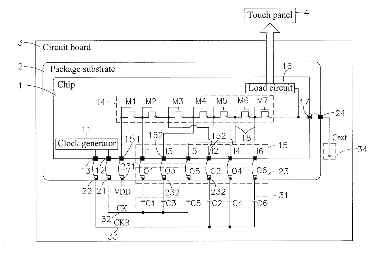
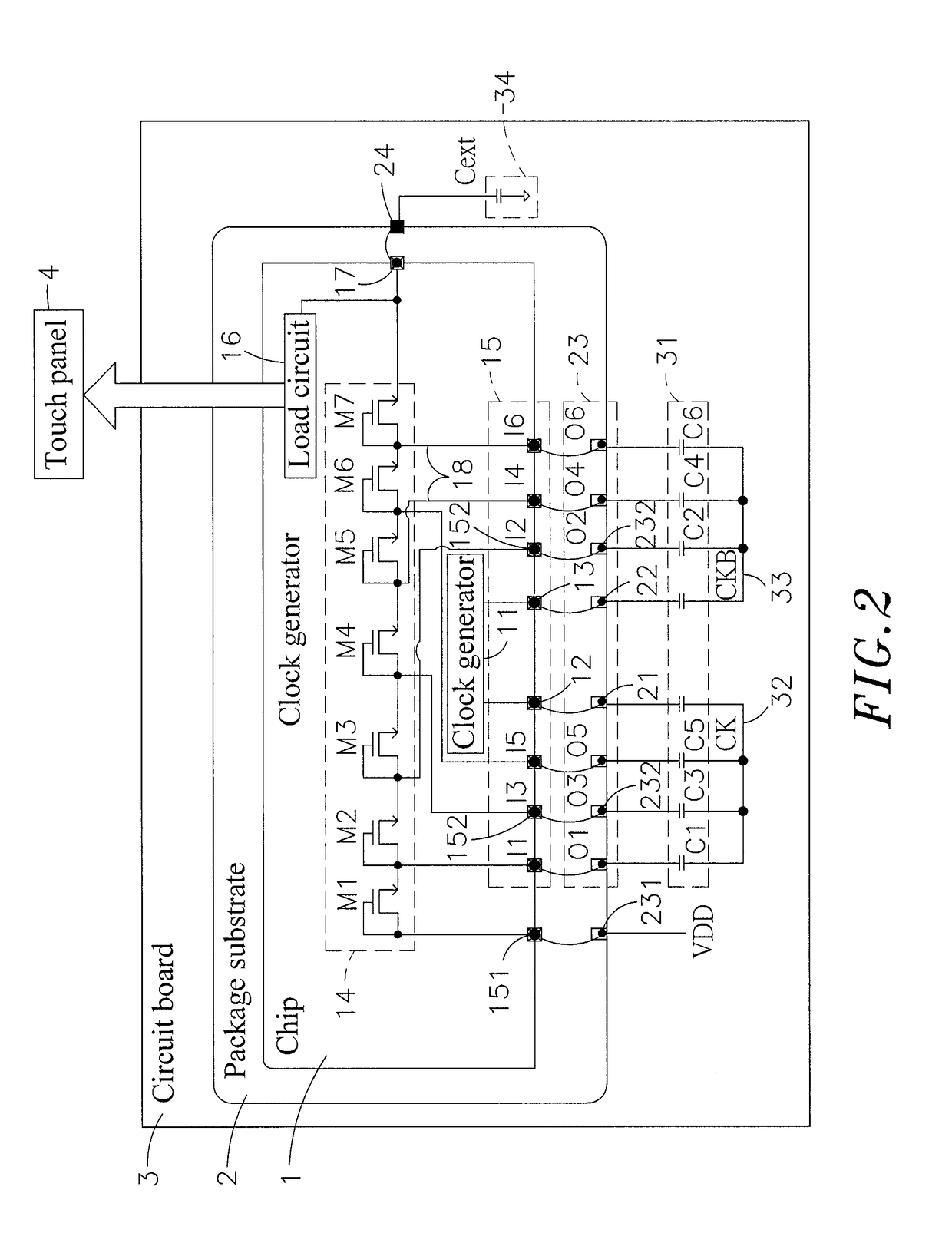
The present invention provides a charge pump that is efficient in operation and avoids negative pulse signal interference. It is achieved by reducing the distance and area of the circuits and the traces in the chip, minimizing parasitic capacitance. The clock generator of the chip is located at one lateral side relative to the transistor set, which allows the second circuit of the circuit board to be located at an outer side relative to the first circuit without being intersected. The at least three second external pins can be disposed adjacent to the first clock pin and the second clock pin, further reducing the distance and area between the first circuit and the second circuit.

Problems solved by technology

Due to creation of the points of intersection Z4 after shunting of the first circuit Z1 and the second circuit Z2, the circuit board Z needs to provide an extra layer for the arrangement of traces, increasing the number of layers and complexity of the structure of the circuit board Z and resulting in increased circuit board cost.
Further, the arrangement of long and large area traces in the circuit board brings relatively larger parasitic capacitance, lowering the charge pump operating efficiency and resulting in negative pulse signal interference.

Method used


Image

  • Charge pump based on a clock generator integrated chip
  • Charge pump based on a clock generator integrated chip
  • Charge pump based on a clock generator integrated chip

Examples


Embodiment Construction

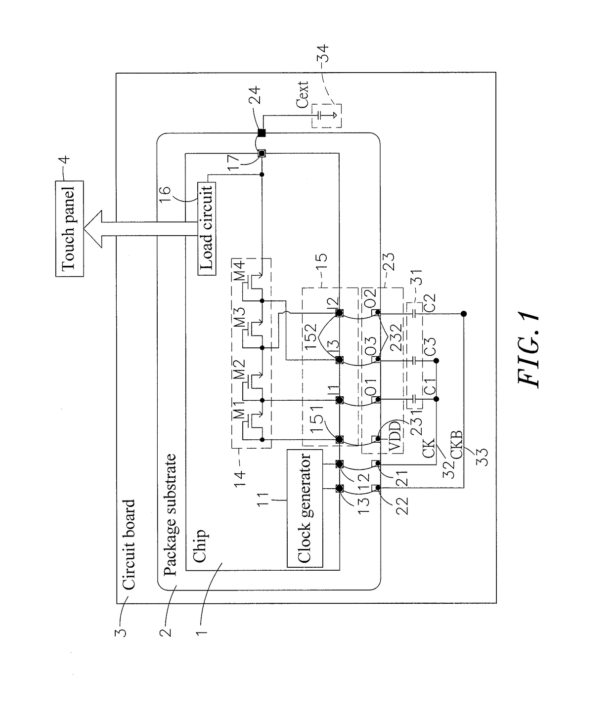
[0016]Referring to FIG. 1, a charge pump in accordance with the present invention is shown. The charge pump comprises a chip 1, a package substrate 2 and a circuit board 3.

[0017]The chip 1 comprises a clock generator 11, a first clock terminal 12 and a second clock terminal 13 respectively and electrically coupled to the clock generator 11, a transistor set 14, an input terminal set 15, a load circuit 16 and an output terminal 17. The clock generator 11 of the chip 1 is electrically coupled with the first clock terminal 12 and the second clock terminal 13 and adapted for generating and outputting a pulse signal CK through the first clock terminal 12 and a negative pulse signal CKB through the second clock terminal 13. The transistor set 14 comprises, for example, but not limited to, four transistors (M1˜M4). The drains of the transistors (M1˜M4) are respectively electrically connected to the respective gates. Further, the connection points between the drains and gates of the transis...


PUM


Abstract

A charge pump includes chip, package substrate and circuit board. Chip includes transistor set including at least four transistors connected to first input end of input terminal set and two rows of odd number and even number second input ends of input terminal set. Except first transistor, the other transistors are arranged in two rows subject to odd number and even number and respectively electrically coupled to the two rows of at least three second input ends by traces. At least three second external pins of package substrate and at least three capacitors of circuit board are respectively arranged in two rows subject to odd number and even number, enabling first circuit with connected odd number second external pins and second circuit with connected even number second external pin to be kept apart without intersection. Traces in chip are arranged in staggered manner, reducing parasitic capacitance.

Description

BACKGROUND OF THE INVENTION[0001]This application claims the priority benefit of Taiwan patent application number 104141341, filed on Dec. 9, 2015.[0002]1. Field of the Invention[0003]The present invention relates to charge pump technology, and more particularly, to a charge pump based on a clock generator integrated chip for use in a touch panel, which has a transistor set of a chip thereof electrically coupled to a first input end and at least three second input ends that are arranged in two rows subject to odd number and even number, and then coupled to a package substrate and a circuit board in a similar arrangement and also electrically coupled to a clock generator, enabling the traces in the chip to be arranged in a staggered manner with the first circuit and second circuit of the circuit board spaced apart without intersection, minimizing generation of parasitic capacitance.[0004]2. Description of the Related Art[0005]A touch panel can be joined with a display screen to creat...

Claims


Application Information

Patent Timeline
Patent Type & Authority Patents(United States)
IPC IPC(8): G05F1/10H01L27/088G05F3/02G06F3/041H02M3/07
CPCH02M3/07H01L27/088G06F3/041H02M3/073H02M3/075G06F3/0416
Inventor LIN, PO-CHUAN
Owner EGALAX EMPIA TECH INC
Why Eureka
Eureka Blog
Learn More