Organic electroluminescent device and manufacturing method thereof
a technology of electroluminescent devices and manufacturing methods, applied in the direction of luminescent screen, discharge tube luminescent screen, instruments, etc., can solve the problems of affecting difficult to apply photolithography, and blunt patterns, and achieve high precision and prevent the effect of bending
- Summary
- Abstract
- Description
- Claims
- Application Information
AI Technical Summary
Benefits of technology
Problems solved by technology
Method used
Image
Examples
example 1
[0062]A 1.1 mm thick alkali-free glass substrate with a 130 nm thick ITO (indium tin oxide) transparent electrode film formed by sputtering on the surface of the glass substrate was cut to a size of 120×100 mm. The ITO substrate was coated with a photoresist, and the laminate was exposed and developed for patterning by ordinary photolithography. The unnecessary portions of ITO were removed by etching, and subsequently the photoresist was removed to form 90 mm long and 80 μm wide stripes from the ITO film in conformity with a predetermined pattern. The stripes were 816 first electrodes disposed at a pitch of 100 μm.
[0063]Then, a positive photoresist (OFPR-800 produced by Tokyo Ohka Kogyo Co., Ltd.) was applied to have a thickness of 3 μm by spin coating on the substrate with the first electrodes formed on it. The coating film formed of the photoresist was exposed pattern-wise through a photo mask and developed to be patterned. The development was followed by curing at 180° C. Thus, t...
example 2
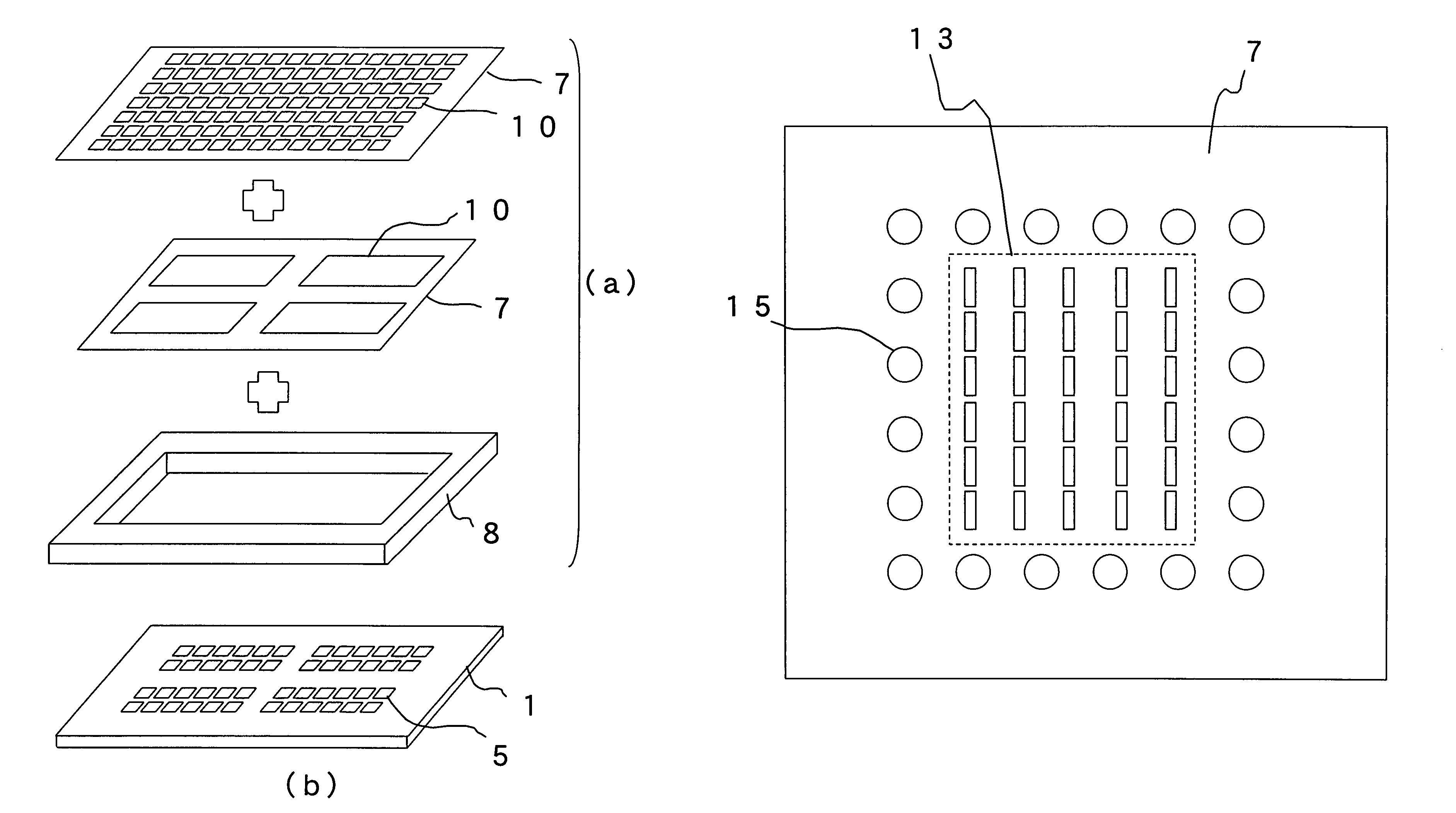
[0076]An organic electroluminescent device was prepared as described in Example 1, except that the deposition mask for the luminescent layer had a effective area consisting of 200 openings in the lengthwise direction and 272 openings in the crosswise direction and that circular dummy openings with a diameter of 200 μm were arranged at a pitch of 400 μm in an area of 3 mm around the effective opening area, as shown in FIG. 10.
[0077]The organic electroluminescent device was driven by line sequential drive, and good display characteristics could be obtained. Further, through a microscope observation to the luminescent pixels, it was confirmed that mixing between adjacent pixels did not occur and that a good luminescent layer pattern could be formed over the entire surface of the luminescent area.
example 3
[0078]A 1.1 mm thick alkali-free glass substrate with a 130 nm thick ITO transparent electrode film formed by sputtering on the surface of the glass substrate was cut to a size of 120×100 mm. The ITO substrate was coated with a photoresist, and the laminate was exposed and developed by ordinary photolithography for patterning. The unnecessary portions of ITO were removed by etching, and subsequently the photoresist was removed to form 90 mm long and 160 μm wide stripes from the ITO film in conformity with a predetermined pattern. Four hundred and eight striped first electrodes were disposed at a pitch of 200 μm.
[0079]Then, a positive photoresist (OFPR-800 produced by Tokyo Ohka Kogyo Co., Ltd.) was applied to have a thickness of 3 μm by spin coating on the substrate having the first electrodes formed on it. The coating film formed of the photoresist was exposed pattern-wise through a photo mask and developed to be patterned. The development was followed by curing at 180° C. Thus, th...
PUM
| Property | Measurement | Unit |
|---|---|---|
| distance | aaaaa | aaaaa |
| width | aaaaa | aaaaa |
| thickness | aaaaa | aaaaa |
Abstract
Description
Claims
Application Information
 - R&D
- Intellectual Property
- Life Sciences
- Materials
- Tech Scout
- Unparalleled Data Quality
- Higher Quality Content
- 60% Fewer Hallucinations
Browse by: Latest US Patents, China's latest patents, Technical Efficacy Thesaurus, Application Domain, Technology Topic, Popular Technical Reports.
© 2025 PatSnap. All rights reserved.Legal|Privacy policy|Modern Slavery Act Transparency Statement|Sitemap|About US| Contact US: help@patsnap.com


