Semiconductor device package

a technology of semiconductor devices and devices, applied in semiconductor devices, semiconductor/solid-state device details, electrical apparatus, etc., can solve the problems of short-time failure of semiconductor chips, decrease in electrical insulation, and adverse effects of semiconductor devices, so as to improve the adhesion and improve the adhesion. , the effect of improving the adhesion

Inactive Publication Date: 2010-07-06
ABLIC INC
View PDF4 Cites 3 Cited by
  • Summary
  • Abstract
  • Description
  • Claims
  • Application Information

AI Technical Summary

Benefits of technology

[0010]A semiconductor device package according to the present invention has a mesh structure in a part of a connecting surface between a lead frame and a resin package body, whereby a connecting area of the connecting surface is increased to enhance a connection between the lead frame and the resin package body. Besides, the three-dimensional mesh structure makes the connecting surface between the lead frame and a resin also three-dimensional to extraordinarily improve the adhesion property there between.
[0011]In addition, the mesh size of the mesh structure is made smaller than an average diameter of filler particles contained in the resin, whereby reducing the number of fillers reaching to the vicinity of a surface of the lead frame. Accordingly, change of an elastic modulus of the resin in the vicinity of the lead frame permits the resin to follow the lead frame deformation by stress from the environment for use of the semiconductor device package, thereby improving adhesion.
[0012]By forming the semiconductor device package with the mesh structure according to the present invention, connecting property between the lead frame to which a semiconductor chip is mounted, and the resin package body can be considerably increased. Moreover, distribution of the fillers contained in the resin can be changed in the vicinity of the lead frame, improving reliability of adhesion between the resin and the connecting surface of the lead frame. Accordingly, separation is less likely to occur in the connecting surface between the lead frame and the resin package body, and infiltration of water and contaminants as well as various associated problems are prevented, whereby improving the quality of the electronic device package.

Problems solved by technology

One of the problems inherent in this type of semiconductor device package is that water infiltrates into the interior thereof along an interface between the resin and the lead frame, resulting in adverse effects such as a decrease in electrical insulation.
The infiltration of water and contaminants induces a short-time failure in the semiconductor chip due to corrosion of a pad.
The water becomes steam and expands, causing package cracks at a high temperature treatment of the electronic device package in the manufacturing process such as board mounting.
Though the conventional plasma cleaning method is effective for an upward exposed surface, the method is, however, less effective in increasing an adhesive force between the back surface of the central die pad portion 107 and the resin package body 104.
In addition, the method has little effects in increasing the adhesive force between the adhesive resin layer and the lead frame.
Moreover, the plasma treatment needs to be performed as a batch treatment, which is uneconomical, and thus the plasma treatment is hard to be applied to assembly process of the resin package production which is continuously performed.
On the other hand, the method of forming on a surface of the lead frame 102 a surface treatment layer made of a black oxide, a brown oxide, a tin oxide and organic silane, or the like is extremely effective for the treatment of inside of the package, but the method causes a number of problems in the treatment of outside of the package.
However, when the resin bleed occurs on the surface of the surface treatment layer made of the black oxide or the like, a tremendously adhesive film is formed due to the interaction between them, which cannot be easily removed.
Complete removal of the resin bleed of the surface treatment layer without damaging the lead frame and the package is extremely difficult.

Method used


Image

  • Semiconductor device package
  • Semiconductor device package
  • Semiconductor device package

Examples


first embodiment

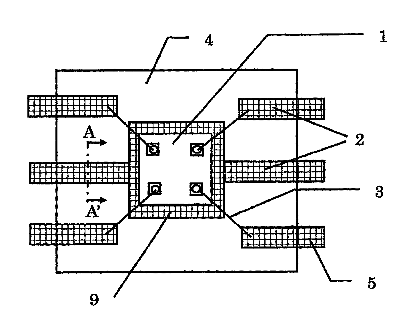
[0023]FIG. 1 shows the present invention. In a semiconductor device package 4, a semiconductor chip 1 is disposed on a die pad 9 which is located in a center of a lead frame 2 made of a copper material, and is bonded to the die pad 9 through an adhesive resin layer. The semiconductor chip 1 is electrically connected to the lead frame 2 through a bonding wire 3. The resin package body 4 which covers the semiconductor chip 1 and the lead frame 2 and is made of an epoxy resin is formed, and the semiconductor chip 1 and the lead frame 2 are sealed in the resin package body 4 thus formed. A part of the lead frame 2 is extended outside the resin package body 4 to serve as an external lead 5, which is used in connection with an external circuit. The point is that the lead frame 2 used in this case has a mesh structure. The mesh structure may exist only on a surface portion of the lead frame 2 and may exist only on the internal part of the lead frame 2.

[0024]As a resin material forming the ...

second embodiment

[0027]FIG. 3 shows the present invention. The mesh structure of the present invention has a mesh size smaller than an average diameter of filler particles 10 contained in a mold resin. When the mesh size is smaller than the average diameter of the fillers 10 contained in the mold resin to be used, a filler particle having a diameter larger than the average diameter cannot penetrate the mesh structure. Accordingly, an amount and diameter of the fillers contained in the mold resin can be changed in the vicinity of the surface of the lead frame 2, and thus an elastic modulus of the mold resin around the lead frame of the mesh structure 11 can be decreased. Consequently, the mold resin follows the deformation of the lead frame due to an external force, whereby separation is less likely to occur in the connecting surface between the mold resin and the lead frame.

third embodiment

[0028]FIG. 4 shows the present invention, which has a structure in which two or more layers of the mesh structure of the lead frame are piled. With this structure, even when the mesh of each layer has a size larger than the average diameter of the filler particles 10, the resultant mesh size completed by piling the mesh structures becomes smaller, and thus a size of the mesh can be designed with respect to an arbitrary particle diameter. Moreover, when the mesh structure is piled to form a multilayer including more than two layers, the resin penetrates into the lead frame and is structurally bonded thereto more firmly. Accordingly, separation is less likely to occur in the connecting surface between the mold resin and the lead frame.


PUM


Abstract

A surface of a lead frame of a semiconductor device package, on which a semiconductor chip is mounted, is formed to have a mesh structure, whereby a connecting area between the lead frame and a molding resin can be increased to have strong bonding. Further, only filler particles having a small diameter than the mesh are taken into the vicinity of the lead frame, suppressing the effect of stresses to reduce deformation of the lead frame.

Description

RELATED APPLICATIONS[0001]This application claims priority under 35 U.S.C. §119 to Japanese Patent Application No. JP2007-195494 filed on Jul. 27, 2007, the entire content of which is hereby incorporated by reference.BACKGROUND OF THE INVENTION[0002]The present invention relates to a semiconductor device package.[0003]A semiconductor device package in which a microelectronic device such as a semiconductor chip is electrically connected to a lead frame and molded with resin is widely used. FIG. 6 shows a structure of a typical semiconductor device package in which a semiconductor chip 101 is disposed on a central die pad portion 107 which is a part of a lead frame 102, and is bonded thereto with an adhesive resin layer. The semiconductor chip 101 is electrically connected to the lead frame 102 through bonding wires 103. A resin package body 104 made of epoxy resin and filler is formed to cover the semiconductor chip 101 and the lead frame 102, sealing the semiconductor chip 101 and t...

Claims


Application Information

Patent Timeline
Patent Type & Authority Patents(United States)
IPC IPC(8): H01L23/495
CPCH01L23/3107H01L23/49537H01L23/49541H01L23/49579H01L2224/48247H01L2224/49171H01L2924/01078H01L24/49H01L24/48H01L2924/14H01L2924/00H01L2224/05554H01L2924/00014H01L2924/10162H01L2224/45099H01L2224/45015H01L2924/207H01L23/488H01L23/495
Inventor KADOI, KIYOAKI
Owner ABLIC INC
Why Eureka
Try Eureka