
Systems and methods for inspecting an edge of a specimen

a specimen and edge technology, applied in the direction of measurement devices, semiconductor/solid-state device testing/measurement, instruments, etc., can solve the problems of untraceable yield loss, catastrophic wafer breakage, cross contamination during processing,

Active Publication Date: 2010-06-01
KLA TENCOR TECH CORP
View PDF23 Cites 24 Cited by
  • Summary
  • Abstract
  • Description
  • Claims
  • Application Information

AI Technical Summary

Benefits of technology

Enables the detection of defects across the entire wafer surface, including both central and edge regions, reducing the need for multiple inspection tools, lowering costs, and increasing manufacturing throughput by using a single system with adjustable parameters for different inspection areas.

Problems solved by technology

The main concerns are that edge defects could fall onto the central part of the wafer thereby causing untraceable yield loss, cross contamination during processing, and / or catastrophic wafer breakage.
These yield loss mechanisms are experienced by most wafer and IC manufacturers at one time or another.
As a result, these large amounts of light will saturate the detectors of traditional wafer inspection systems.
Consequently, any output signals generated near or at the edge of wafers by such wafer inspection tools are generally unusable.
However, some edge inspection systems have been developed to detect defects at or near the edge of wafers.
Therefore, the edge inspection systems are not optimized to, or even able to, detect defects in the central region of the wafers.
Consequently, if wafer or IC manufacturers want to detect defects in both the central and outer regions of wafer (as is usually the case since defects in either region may result in expensive yield losses and other problems), they will need to purchase two separate tools.
Using two different wafer inspection tools instead of just one inspection tool will obviously increase costs in many ways such as increases in clean room real estate costs, operating costs, tool maintenance costs, and reduced throughput.
However, since most inspection tools are not capable of inspecting both the inner region and edge of wafers, and due to the increasing costs associated with defect-based yield losses, wafer and IC manufacturers may not be able to avoid the costs associated with multiple, different inspection tools.
In addition, incorporating an additional subsystem into an existing inspection tool will also increase the overall cost of the tool due to the hardware and possibly software required for the additional inspection subsystem and increased maintenance costs for the additional subsystem.

Method used


Image

  • Systems and methods for inspecting an edge of a specimen
  • Systems and methods for inspecting an edge of a specimen
  • Systems and methods for inspecting an edge of a specimen

Examples


Embodiment Construction

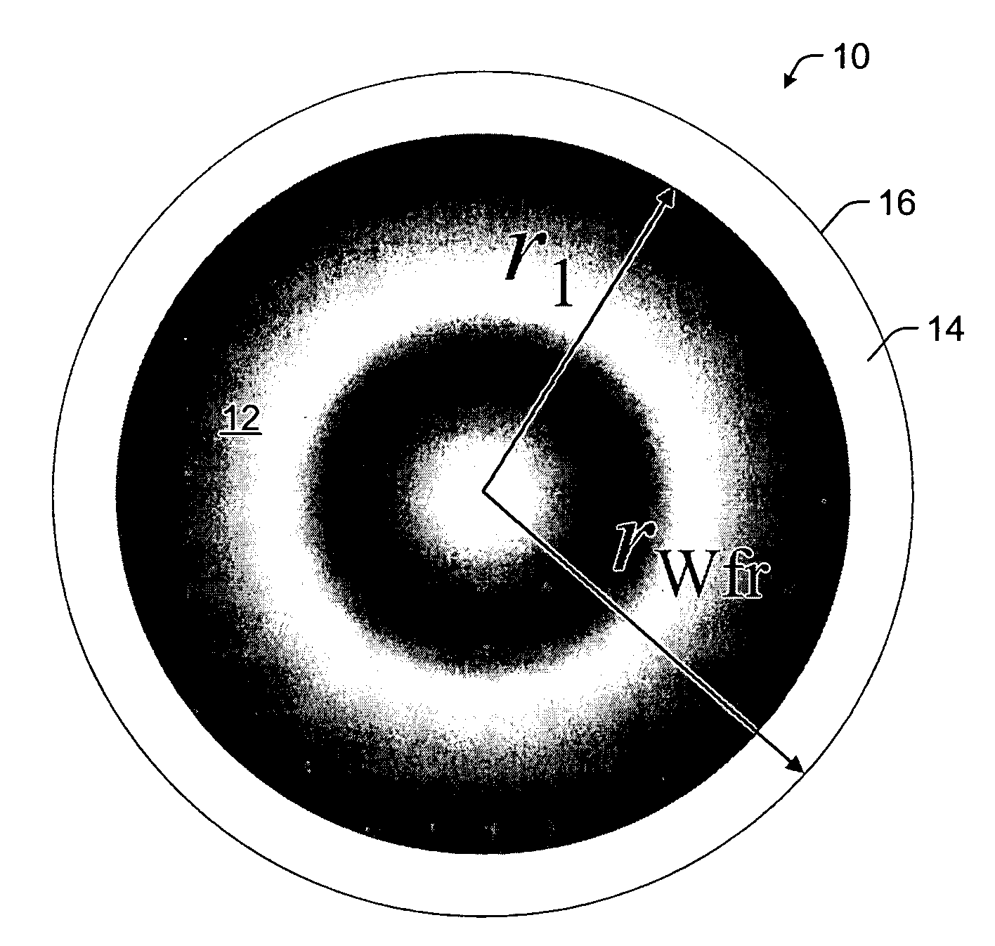
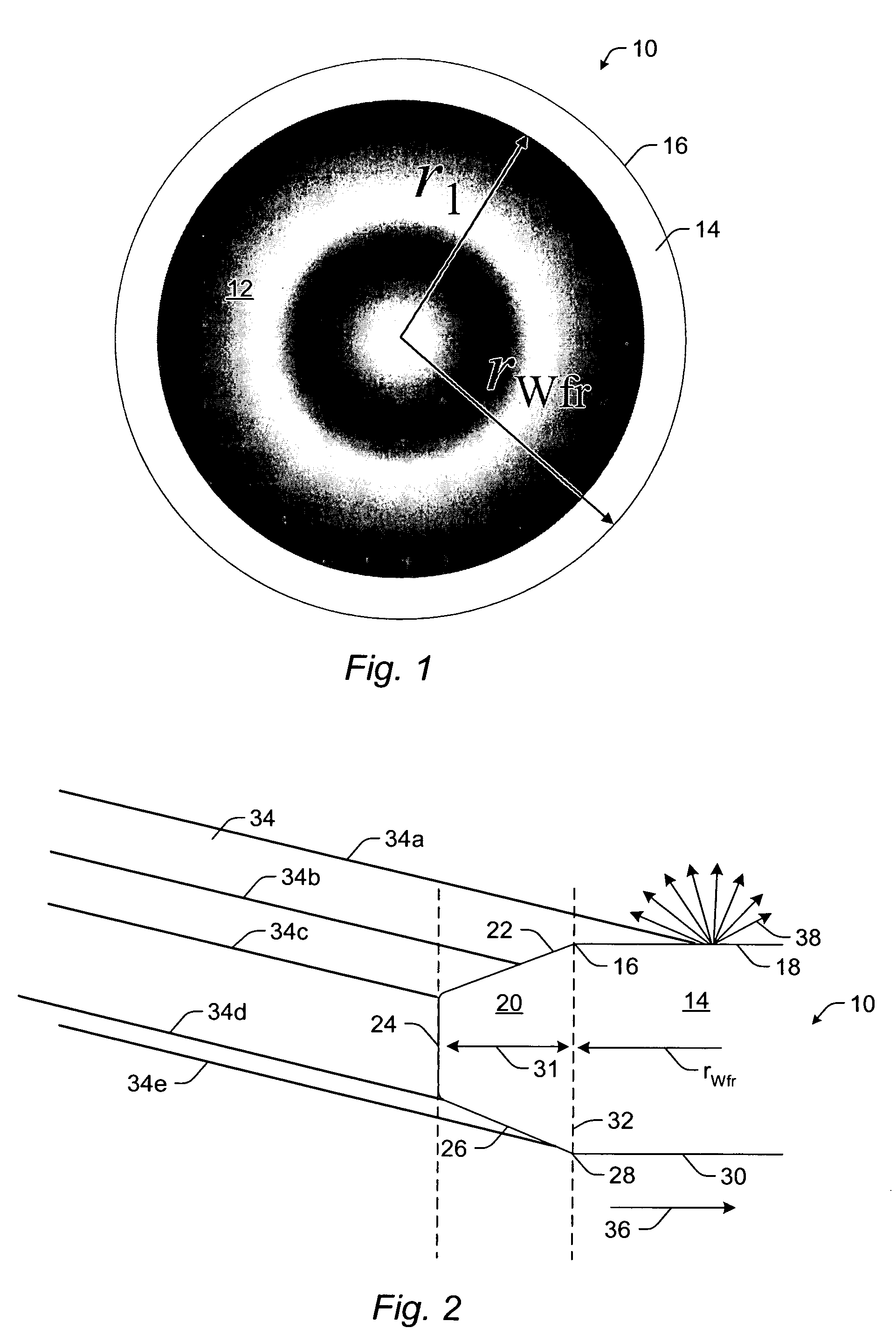
[0030]As used herein, the term “specimen” generally refers to a wafer or any other specimen having an edge on which defects of interest may be located. Although the terms “specimen” and “wafer” are used interchangeably herein, it is to be understood that embodiments described with respect to a wafer may configured and / or used for inspection of any other specimen as described above.

[0031]As used herein, the term “wafer” generally refers to substrates formed of a semiconductor or non-semiconductor material. Examples of such a semiconductor or non-semiconductor material include, but are not limited to, monocrystalline silicon, gallium arsenide, and indium phosphide. Such substrates may be commonly found and / or processed in semiconductor fabrication facilities.

[0032]One or more layers may be formed upon a wafer. For example, such layers may include, but are not limited to, a resist, a dielectric material, and a conductive material. Many different types of such layers are known in the ar...


PUM

PropertyMeasurementUnit
distanceaaaaaaaaaa
angle of incidenceaaaaaaaaaa
sizeaaaaaaaaaa

Abstract

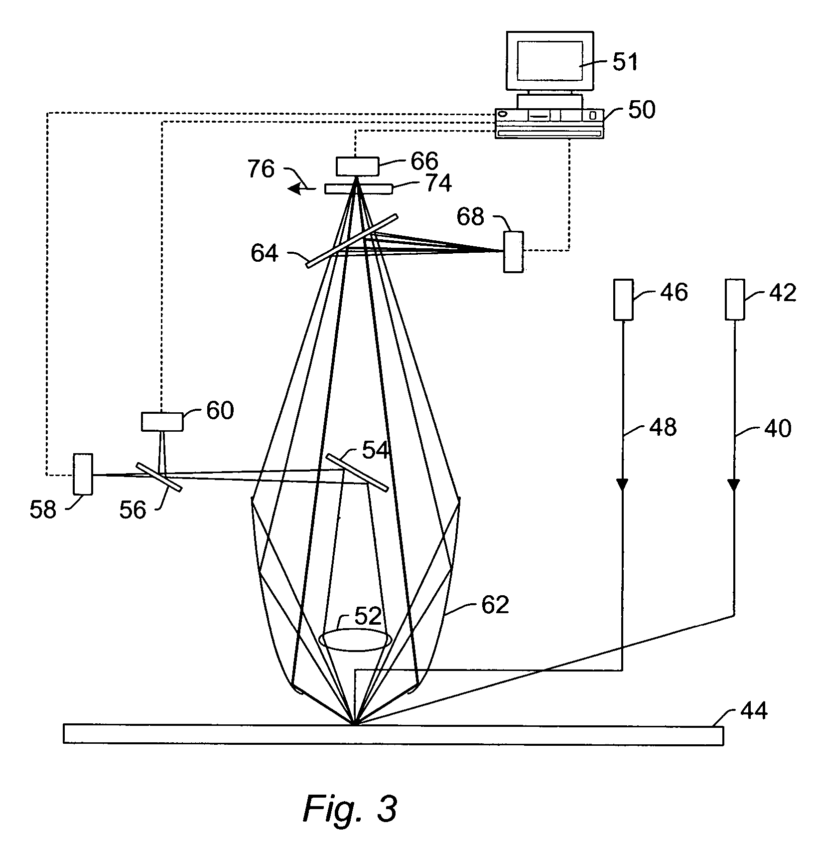
Systems and methods for inspecting an edge of a specimen are provided. One system includes an illumination subsystem configured to direct light to the edge of the specimen at an oblique angle of incidence. The plane of incidence of the light is substantially perpendicular to a plane substantially tangent to the edge of the specimen. The system also includes a detection subsystem configured to collect light scattered from the edge and to generate signals responsive to the scattered light. One method includes directing light to the edge of the specimen at an oblique angle of incidence. The plane of incidence is substantially perpendicular to a plane substantially tangent to the edge of the specimen. The method also includes collecting light scattered from the edge and generating signals responsive to the scattered light. The signals described above can be used to detect defects on the edge of the specimen.

Description

BACKGROUND OF THE INVENTION[0001]1. Field of the Invention[0002]The present invention generally relates to systems and methods for inspecting an edge of a specimen. Certain embodiments relate to a system that includes an illumination subsystem that is configured to direct light to the edge of the specimen at an oblique angle of incidence.[0003]2. Description of the Related Art[0004]The following description and examples are not admitted to be prior art by virtue of their inclusion in this section.[0005]Fabricating semiconductor devices such as logic and memory devices typically includes processing a specimen such as a semiconductor wafer using a number of semiconductor fabrication processes to form various features and multiple levels of the semiconductor devices. For example, lithography is a semiconductor fabrication process that typically involves transferring a pattern to a resist arranged on a semiconductor wafer. Additional examples of semiconductor fabrication processes inclu...

Claims


Application Information

Patent Timeline
Patent Type & Authority Patents(United States)
IPC IPC(8): G01N21/00
CPCG01N21/8806G01N21/9501H01L22/12G01N21/9503G01N21/95623G01N2021/8822
Inventor HALLER, KURT LINDSAYCUI, STEVE YIFENGLERA, JARED
Owner KLA TENCOR TECH CORP
Learn More