Apparatus and method for monitoring processing of a substrate

a substrate and substrate technology, applied in the field of semiconductor wafer processing systems, can solve the problems of substrate, electrical charge leakage, substrate, insulating layer and/or resultant circuit pattern damage, etc., and achieve the effect of simplifying the overall design

Inactive Publication Date: 2009-12-15
APPLIED MATERIALS INC
View PDF48 Cites 16 Cited by
  • Summary
  • Abstract
  • Description
  • Claims
  • Application Information

AI Technical Summary

Benefits of technology

[0014]With the method and apparatus as disclosed, process measurement and monitoring is conducted without encountering interference from high power energy sources proximate the chamber. Specifically, the monitoring assembly is positioned away from RF power sources that can arbitrarily couple power into the monitoring assembly. Additionally, the line-of-sight feature of the subject invention simplifies the overall design and allows retrofitting of chambers not previously using such in-situ monitoring devices. The apparatus further provides versatility since the removable window allows interchanging different types of monitoring apparatus. Specifically, plasma-based lamps, laser interferometers, X-ray emitters and the like are optimized by selecting different types of window material (i.e., sapphire, quartz and the like) through which monitoring beams propagate.

Problems solved by technology

Minute changes in the composition or pressure of an etch gas or process chamber or wafer temperature creates undesirable etch results.
Otherwise, the information is not sustained (i.e., the electrical charge “leaks out” of the storage cell).
It can easily be seen that if the etch process during any one step exceeds the predetermined endpoint, the substrate, insulating layer and / or resultant circuit pattern may be damaged.
Unfortunately such monitoring and measuring systems are plagued by inadequate signal to noise ratios.
Additionally, the minimum etch depth is limited by the wavelength of the light source used in the monitor.
Unfortunately, the error in etch depth detection in systems that use polarized laser beams too great to be useful.
However, the RF power may inductively couple into the neighboring monitoring equipment thereby corrupting the monitoring signals.
As such, in situ monitoring of etch depth in a high power RF environment is inadequate and prone to severe inaccuracy.

Method used


Image

  • Apparatus and method for monitoring processing of a substrate
  • Apparatus and method for monitoring processing of a substrate
  • Apparatus and method for monitoring processing of a substrate

Examples


Embodiment Construction

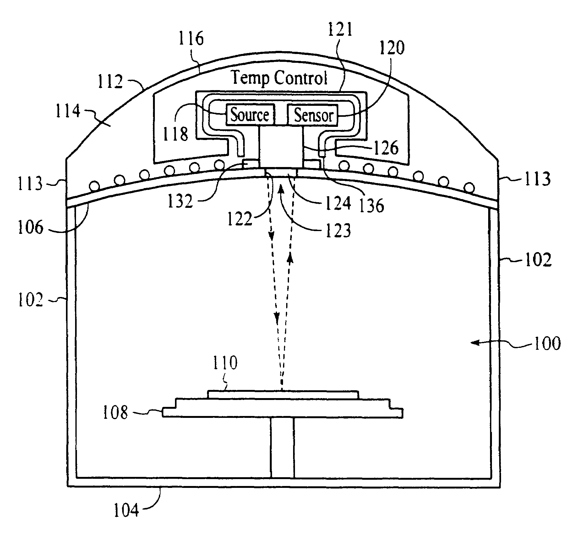
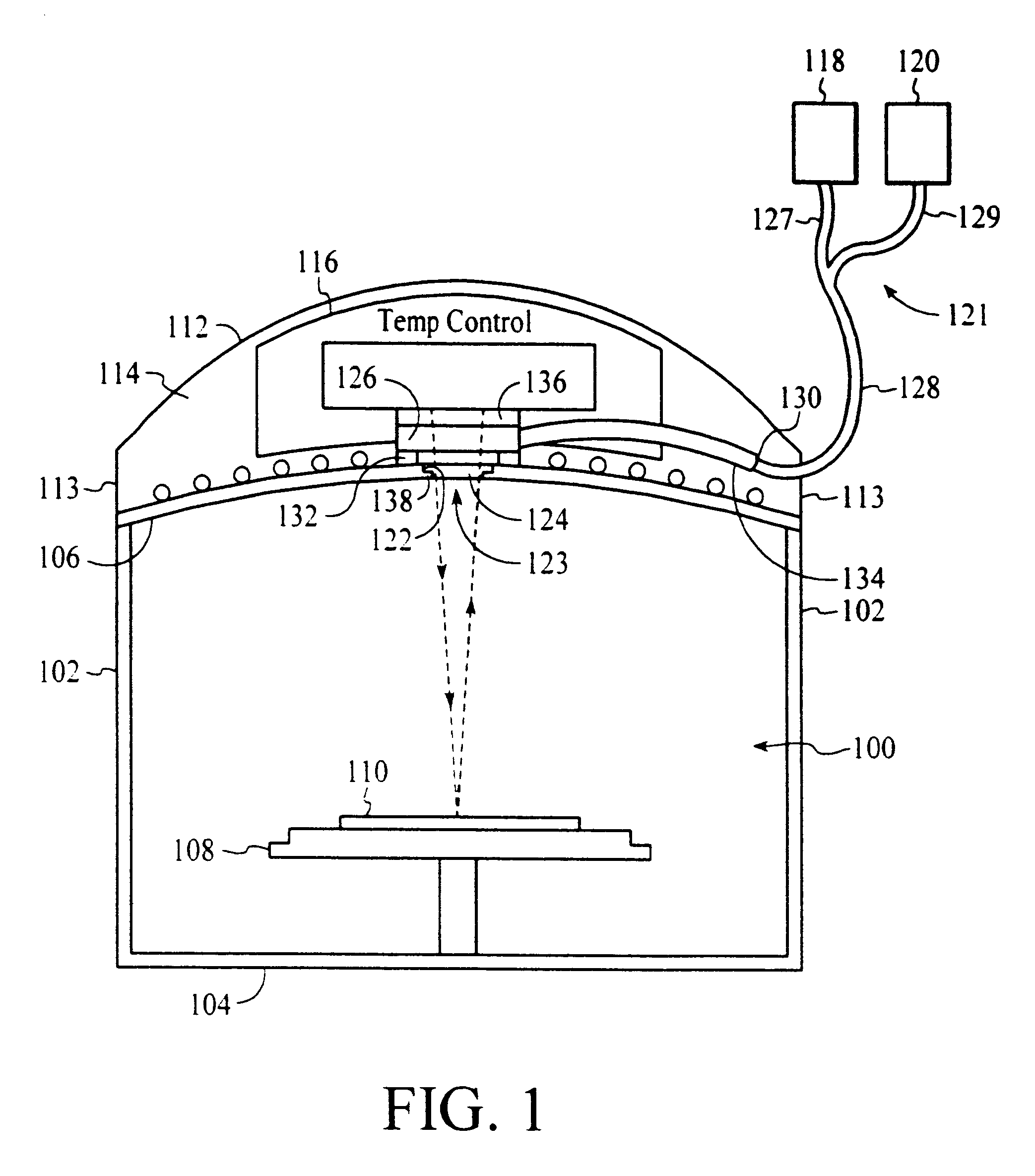
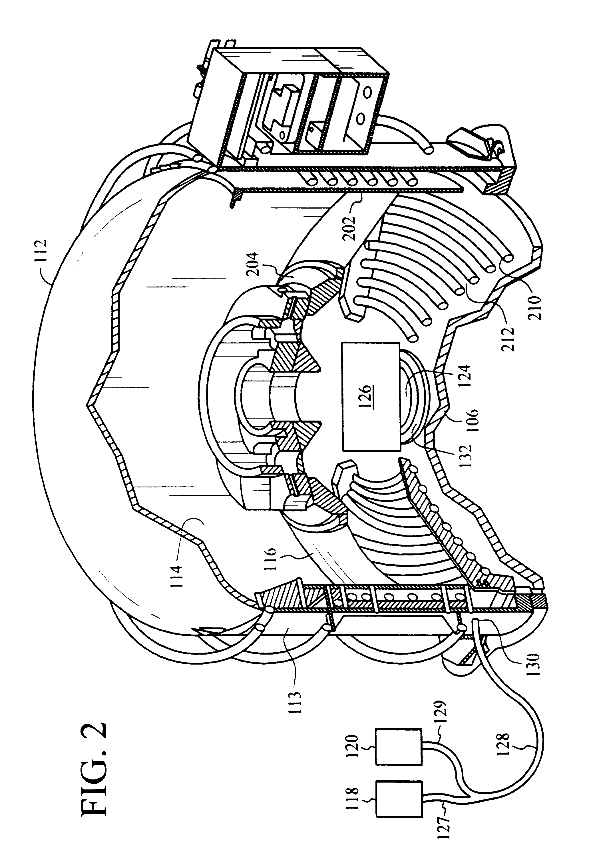
[0023]The present invention is an apparatus for performing direct, in situ monitoring of processes such as etch depth of and thin film deposition upon a semiconductor wafer within a semiconductor wafer processing system. The invention provides for measurement of a variety of emissia or reflected light dependent upon chamber conditions and monitoring apparatus preferences and parameters. Specifically, the invention is used for monitoring the depth of various types of etch processes from within a dome temperature control enclosure of a Metal Etch Decoupled Plasma Source (DPS) chamber manufactured by Applied Materials of Santa Clara, Calif. A dome temperature control enclosure and apparatus of the Metal Etch DPS chamber is disclosed in U.S. patent application Ser. No. 08 / 767,071 filed Dec. 16, 1996 and is herein incorporated by reference. The processes that can be monitored include but are not limited to gate etch, recess etch, deep trench and shallow trench isolation for the productio...


PUM

PropertyMeasurementUnit
Poweraaaaaaaaaa
Radiusaaaaaaaaaa
Depthaaaaaaaaaa

Abstract

Apparatus for in-situ monitoring of a process in a semiconductor wafer processing system consists of a process chamber having a dome, an enclosure disposed above the chamber, a process monitoring assembly positioned proximate the dome, an opening in the dome, and a window covering the opening. A portion of the apparatus supports the process monitoring assembly to establish a line-of-sight propagation path of monitoring beams from above the dome, through the window to the substrate to facilitate etch depth measurement without encountering interference from high power energy sources proximate the chamber. A method of fabricating a process monitoring apparatus consists of the steps of boring an opening into a dome, positioning the process monitoring assembly in proximity to the dome so as to allow a line-of-sight propagation path of monitoring beams from the process monitoring assembly to a wafer, and covering the opening with a window. The window is permanent or removable dependent upon the type of process monitoring assembly being used in the system.

Description

CROSS-REFERENCE[0001]This application is a divisional of U.S. patent application Ser. No. 08 / 944,240, filed on Oct. 6, 1997 now U.S. Pat. No. 6,129,807, which is incorporated herein by reference in its entirety.BACKGROUND OF THE DISCLOSURE[0002]1. Field of the Invention[0003]The invention relates to semiconductor wafer processing systems.[0004]2. Description of the Background Art[0005]Semiconductor processing systems that perform “dry” etching of semiconductor wafers via plasmic gases, also known as reactive ion etching (RIE) require constant monitoring. While it is possible to predefine the etch parameters and allow the systems to perform the etch process unmonitored, conditions within the systems can change over time. Minute changes in the composition or pressure of an etch gas or process chamber or wafer temperature creates undesirable etch results.[0006]For example, DRAM memory circuits are fabricated from semiconductor wafers using deep trench technology. A single DRAM memory c...

Claims


Application Information

Patent Timeline
IPC IPC(8): G01J3/00H01L21/00H01J37/32H01L21/302H01L21/3065
CPCH01J37/32935H01J37/32458
Inventor GRIMBERGEN, MICHAELPAN, SHAOHER X.
Owner APPLIED MATERIALS INC
Why Eureka
Try Eureka